Semiconductor device and manufacturing method thereof

A manufacturing method and semiconductor technology, which is applied in the direction of semiconductor devices, transistors, electrical components, etc., can solve the problems of narrow constant current range and low constant current, and achieve the effects of saving chip area, stable current value, and good specific withstand voltage

Inactive Publication Date: 2016-03-16
UNIV OF ELECTRONICS SCI & TECH OF CHINA
View PDF3 Cites 14 Cited by
  • Summary
  • Abstract
  • Description
  • Claims
  • Application Information

AI Technical Summary

Problems solved by technology

However, the current constant current devices are still turned on when the reverse voltage is applied, and the range of the constant current region is generally narrow, and the constant current that can be provided is also low.

Method used


Image

  • Semiconductor device and manufacturing method thereof
  • Semiconductor device and manufacturing method thereof
  • Semiconductor device and manufacturing method thereof

Examples


Embodiment

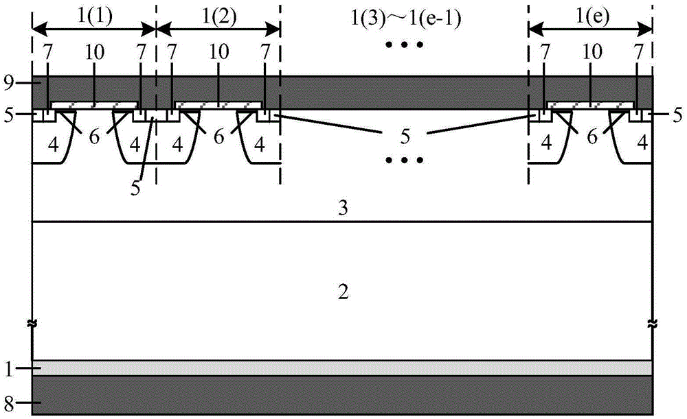
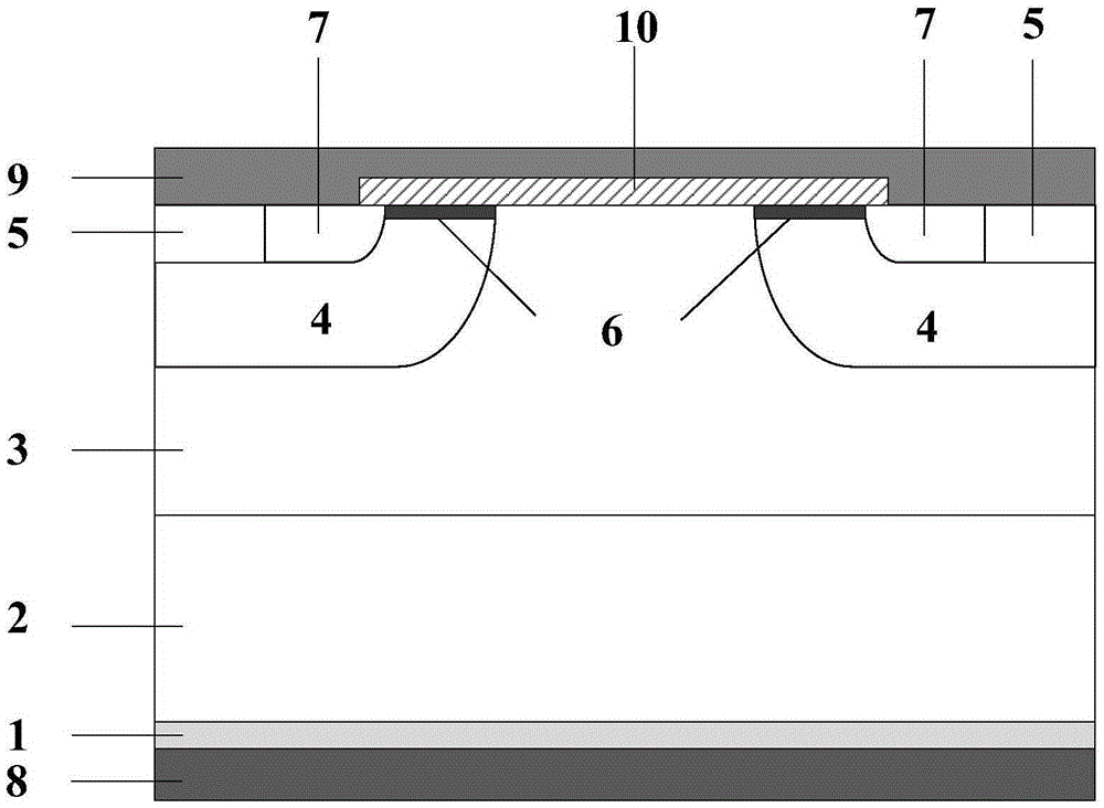
[0049] This embodiment takes a semiconductor device with a forward withstand voltage of about 250V, a current of about 2E-5A / μm, and a reverse withstand voltage of about 450V as an example to describe the technical solution of the present invention in detail.

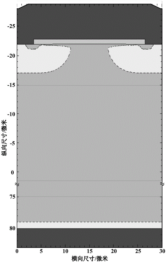
[0050] With the help of TSUPREM4 and MEDICI simulation software for example figure 2 The process simulation of the cells of the semiconductor device shown is carried out. The simulation parameters are: the thickness of the initial silicon wafer is about 250 μm, the resistivity of the N-type doped substrate 2 is 10-20Ω·cm, and the thickness of the N-type lightly doped epitaxial layer 3 is 22 μm; the depth of the two symmetrical diffused P-type well regions 4 is about 4-6 μm, and the width is about 10-12 μm, and the two diffused P-type well regions 4 are implanted with boron, and the distance between them is about 8 μm; Phosphorus is injected into the channel Adjustable ions; the first P-type heavily doped region 5 used ...


PUM


Abstract

The invention discloses a semiconductor device and a manufacturing method thereof, and belongs to the technical field of semiconductors. The semiconductor device comprises a plurality of cells which are the same in structure and are sequentially connected with one another, wherein each cell comprises an N-type doped substrate, an N-type lightly doped epitaxial layer, a diffused P-type well region, a first P-type heavily dope region, an N-type heavily dope region, an oxidation layer, a metal cathode, a second P-type heavily doped region and a metal anode; the N-type lightly doped epitaxial layer is located on the N-type doped substrate; the diffused P-type well region is located in the N-type lightly doped epitaxial layer; the first P-type heavily dope region and the N-type heavily dope region are located in the diffused P-type well region; the oxidation layer is located on the upper surfaces of the N-type lightly doped epitaxial layer and the diffused P-type well region; the metal cathode covers the overall cells; and the second P-type heavily doped region and the metal anode are located on the lower surface of the N-type doped substrate. According to the semiconductor device disclosed by the invention, a semiconductor material which is opposite to the substrate in the doping type is injected into the back surface of the substrate, so that, on one hand, holes are injected into the N-type substrate and the N-type lightly doped epitaxial layer through P-type heavily doped back injection, the semiconductor device has two carrier currents, namely a hole current and an electron current, and the current density of the device is increased; and on the other hand, the reverse withstand voltage of the device can be improved.

Description

technical field [0001] The invention belongs to the technical field of semiconductors, and in particular relates to a semiconductor device and a manufacturing method thereof. Background technique [0002] The constant current source is a commonly used electronic equipment and device, and it is widely used in electronic circuits. The constant current source is used to protect the entire circuit, even if the voltage is unstable or the load resistance changes greatly, it can ensure the stability of the supply current. A constant current diode (CRD, Current Regulative Diode) is a semiconductor constant current device, which uses a two-terminal junction field effect transistor as a constant current source instead of an ordinary constant current source composed of multiple components such as transistors, voltage regulator tubes, and resistors. It can maintain a constant current value within a certain working range. When it works in the forward direction, it is a constant current ...

Claims


Application Information

Patent Timeline
Patent Type & Authority Applications(China)
IPC IPC(8): H01L29/73H01L29/06
CPCH01L29/73H01L29/0603
Inventor 乔明方冬于亮亮何逸涛张波
Owner UNIV OF ELECTRONICS SCI & TECH OF CHINA
Why Eureka
Try Eureka