
Matrix anodes manufactured by high temperature co-fired multilayer ceramic technology and method thereof

A technology of multi-layer ceramics and high-temperature co-firing, which is applied to the manufacture of electron multiplier anode devices, multiplier electrodes, and cold cathodes. Good consistency, high production efficiency, and the effect of improving unevenness

Active Publication Date: 2016-03-23
NO 55 INST CHINA ELECTRONIC SCI & TECHNOLOGYGROUP CO LTD
View PDF4 Cites 4 Cited by
  • Summary
  • Abstract
  • Description
  • Claims
  • Application Information

AI Technical Summary

Problems solved by technology

[0007] However, using the metal glass sealing process to make matrix anodes can achieve a higher matrix density, but relatively speaking, the higher the density, the higher the precision requirements for the sealing mold will be. Once the mold is set
[0008] If the design is not well made, some lead-out pins are prone to air leakage, which will lead to a significant decrease in the sealing yield

Method used


Image

  • Matrix anodes manufactured by high temperature co-fired multilayer ceramic technology and method thereof
  • Matrix anodes manufactured by high temperature co-fired multilayer ceramic technology and method thereof
  • Matrix anodes manufactured by high temperature co-fired multilayer ceramic technology and method thereof

Examples


Embodiment

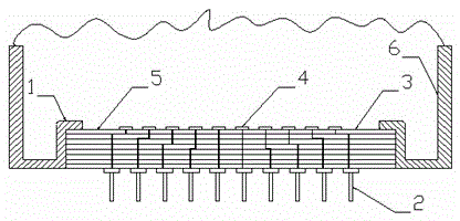
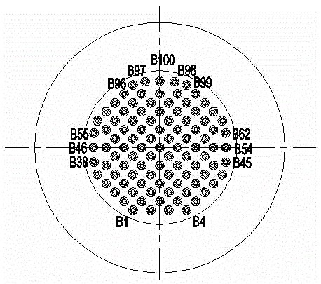
[0047] control figure 1, a 10×10 matrix anode made by high-temperature co-fired multilayer ceramic technology, including: Kovar sealing disc 1; Kovar pin 2; The transition piece between the substrate 3 and the shell is brazed with the multilayer ceramic substrate 3 and sealed with the shell by laser welding or argon arc welding. The multi-layer ceramic substrate 3 is located on the inner surface of the vacuum chamber. On the inner surface of the vacuum chamber is a 10×10 metal contact array 4 uniformly arranged to form an anode input array. On the outer surface of the vacuum chamber is a uniformly arranged 10×10 metal contact array 4. 10 leads out the pin 2 to form an anode output array.

[0048] A method for manufacturing a microchannel plate photomultiplier tube matrix anode using a high-temperature co-fired multilayer ceramic process, comprising:

[0049] Step 1: According to Figure 2, process the Kovar sealing disc 1 with an outer diameter of Φ35.5mm and a height of 2.5m...


PUM

PropertyMeasurementUnit
Thicknessaaaaaaaaaa

Abstract

The invention provides matrix anodes manufactured by a high temperature co-fired multilayer ceramic technology and a method thereof. The structure is that a kovar sealing flange is arranged between a matrix anode multilayer ceramic substrate and a tube shell. The kovar sealing flange is connected with the matrix anode multilayer ceramic substrate. The kovar sealing flange is connected with the tube shell. The surface, which is arranged in the internal part of a vacuum chamber, of the matrix anode multilayer ceramic substrate is composed of xXx metal contact arrays which are uniformly arranged so that anode input arrays are formed. The surface, which is arranged at the external part of the vacuum chamber, of the matrix anode multilayer ceramic substrate is composed of xXx lead-out pins which are uniformly arranged so that anode output arrays are formed. Advantages are that metal lines can be printed on each layer of the substrate, interconnected wiring is performed via vertically metalized through holes, the distance between the electrodes of the two sides of the substrate can be different through manufacturing, and the extremely small physical size of the metal electrodes and electrode insulation clearance can be realized so that the matrix anodes of higher density can be realized; and a semiconductor manufacturing technology is adopted, and consistency of the manufactured matrix anodes is better than that of the matrix anodes manufactured through the conventional technology so that non-uniformity of anode response can be improved and production efficiency can be enhanced.

Description

technical field [0001] The invention relates to a high-temperature co-fired multilayer ceramic process for manufacturing a matrix anode of a microchannel plate photomultiplier tube and a method thereof. The invention belongs to the technical field of electric vacuum photodetection devices. Background technique [0002] The matrix anode microchannel plate photomultiplier tube is a photoelectric conversion detection device that can convert weak optical signals into electrical signals. It has the characteristics of extremely high electronic gain and sensitivity, ultra-fast time response, and ultra-high timing accuracy. Through The follow-up signal readout circuit can realize photon counting and position imaging functions, and can be widely used in laser radar, medical high-resolution gamma camera, high-energy particle detection and other application fields. This type of device is mainly composed of a photocathode, a microchannel plate, a matrix anode and a tube shell with vacu...

Claims


Application Information

Patent Timeline
IPC IPC(8): H01J43/12H01J9/14
CPCH01J9/148H01J43/12
Inventor 杨杰李永彬赵文锦
Owner NO 55 INST CHINA ELECTRONIC SCI & TECHNOLOGYGROUP CO LTD
Learn More