Efficient perovskite solar cell and preparation method thereof
A solar cell and perovskite technology, applied in circuits, photovoltaic power generation, electrical components, etc., can solve problems such as limiting the wide application of perovskite cells, being sensitive to components such as water and oxygen, and destroying device stability, and achieving good application prospects. , low cost, the effect of improving important performance parameters
- Summary
- Abstract
- Description
- Claims
- Application Information
AI Technical Summary
Problems solved by technology
Method used
Image
Examples
preparation example Construction
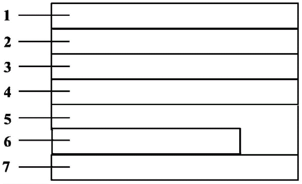
[0034] The present invention also provides a method for preparing the above-mentioned high-efficiency perovskite solar cell, the specific preparation steps are as follows:
[0035] Step 1: Wash the conductive substrate through the traditional substrate cleaning process (ethanol, acetone, isopropanol alternate ultrasonic 10-60min), blow dry with nitrogen for later use;
[0036] Step 2: Deposit a semiconductor oxide transport layer on the conductive substrate treated in step 1 to collect and transport electrons or holes. The deposition thickness is 10-200nm, the deposition temperature is 10-300°C, and the annealing temperature is 300-500°C for sealing save;
[0037] Step 3: Prepare a layer of insulating buffer layer by deposition method on the conductive substrate deposited with electron transport layer after step 2; wherein, the material of the insulating buffer layer is Al 2 o 3 , ZrO 2 , SiO 2 , MgO, Ga 2 o 3 , ZrO 2 , Nb 2 o 5 、 Ta 2 o 5 or HfO 2 . The thickness...
example 1
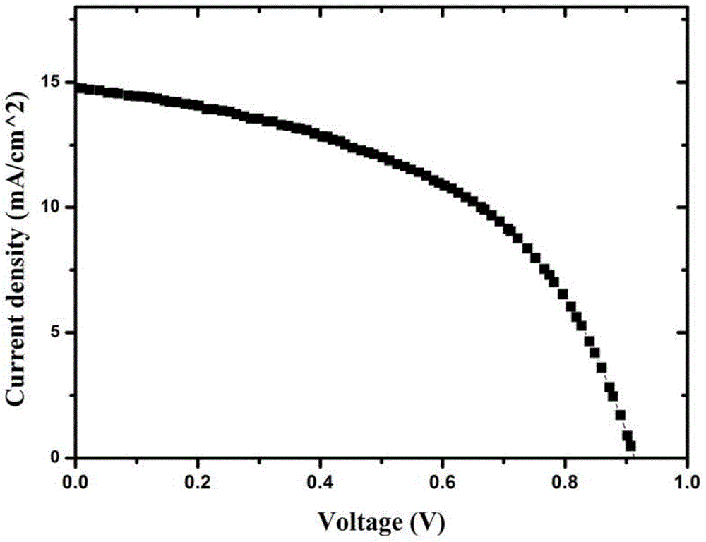
[0048] Example 1: ZnO-based perovskite solar cells (without introducing an insulating buffer layer)
[0049] Clean the conductive glass substrate (FTO / ITO) with high light transmittance, alternately ultrasonicate ethanol, acetone, and isopropanol for 10-60 minutes, and dry it with nitrogen gas for later use. Treat the conductive base by wet etching to obtain the target pattern of the transparent substrate. The n-type semiconductor oxide film (ZnO film) is prepared by magnetron sputtering technology to collect and transmit electrons. The deposition thickness is 10-200nm, the deposition temperature is 10-300°C, and the annealing temperature is 300-500°C for sealed storage.
[0050] TiO 2 The diluted slurry made of particles, the dilution ratio is 1:10, the spin coating speed is 2500rpm-5500rpm, and the high temperature annealing is 300-600℃. After cooling, spin-coat PbX with a concentration of 300-600mg / ml 2 (dissolved in dimethylformamide), dissolved at 70°C for 10-24h until...
example 2
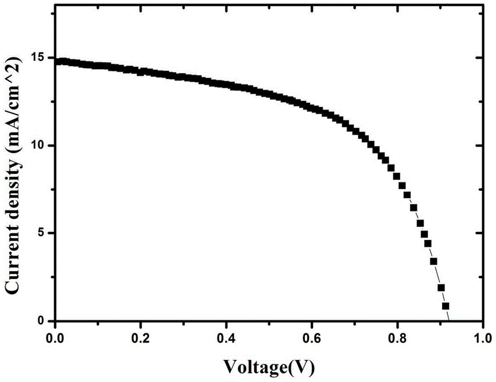
[0051] Example 2: ZnO-based perovskite solar cells (insulating buffer layer introduced)
[0052] Clean the conductive glass substrate (FTO / ITO) with high light transmittance, alternately ultrasonicate ethanol, acetone, and isopropanol for 50 minutes, and dry it with nitrogen gas for later use. Treat the conductive base by wet etching to obtain the target pattern of the transparent substrate. The n-type semiconductor oxide thin film (ZnO thin film) was prepared by magnetron sputtering technology to collect and transmit electrons. The deposition thickness was 50nm, the deposition temperature was 50°C, and the annealing temperature was 300°C for sealed storage.
[0053] TiO 2 The diluted slurry made of particles, the dilution ratio is 1:5, the spin coating speed is 5500rpm, and the high temperature annealing is at 500°C. After cooling, spin-coat PbX with a concentration of 460mg / ml 2 (dissolved in dimethylformamide), dissolved at 70°C for 10h until completely dissolved, and th...
PUM
 Abstract
Description
Claims
Application Information


