Thin film crystalline silicon perovskite heterojunction solar cell and preparation method thereof

A solar cell and perovskite technology, applied in circuits, photovoltaic power generation, electrical components, etc., can solve the performance limitations of solar cell devices such as open circuit voltage, battery efficiency decline, short circuit between perovskite layer and conductive substrate, etc.

Active Publication Date: 2016-03-30
HEBEI UNIV OF TECH
View PDF5 Cites 4 Cited by
  • Summary
  • Abstract
  • Description
  • Claims
  • Application Information

AI Technical Summary

Problems solved by technology

CN201410568822.X discloses an all-solid-state perovskite microcrystalline silicon composite solar cell and its preparation method, but it has the following disadvantages: first, the deposition rate of microcrystalline silicon is relatively slow, generally no more than 5 angstroms per second, and the deposition rate affects production efficiency and cost
Compared with crystalline silicon materials, the recombination of photogenerated carriers inside microcrystalline silicon limits the performance of solar cell devices made of microcrystalline silicon materials such as open circuit voltage.
[0003] The P-type crystalline silicon thin film layer of the thin-film crystalline silicon perovskite heterojunction solar cell in the prior art has a large number of surface states, which causes significant electron-hole recombination at the PN junction interface, and forms a PN junction leakage current macroscopically.
In addition, in long-term operation, the P-type crystalline silicon film is in direct contact with the perovskite material, and impurities on the grain boundaries of the perovskite material and other impurities such as water vapor will diffuse into the crystalline silicon film, resulting in a decrease in battery performance.
In addition, due to the objective actual process manufacturing errors and stress deformation caused by high-temperature treatment in its preparation, in thin-film crystalline silicon perovskite heterojunction solar cells with a thickness of only tens of nanometers to tens of micrometers, its composition There are discontinuities in the actual preparation among the conductive substrate, P-type crystalline silicon film, perovskite layer, electron transport layer and the functional layers of the back electrode, resulting in the actual preparation of thin film crystalline silicon perovskite heterojunction solar cells There is direct contact between the perovskite layer and the conductive substrate, the direct contact between the P-type crystalline silicon film layer and the electron transport layer, the direct contact between the P-type crystalline silicon film layer and the back electrode, and the direct contact between the conductive substrate and the back electrode, which may cause The perovskite layer in the battery is short-circuited with the conductive substrate, the P-type crystalline silicon thin film layer is short-circuited with the electron transport layer, or even the conductive substrate is short-circuited with the back electrode, which causes the efficiency of electron injection into the external circuit to decrease and the battery efficiency to decrease.

Method used


Image

  • Thin film crystalline silicon perovskite heterojunction solar cell and preparation method thereof

Examples


Embodiment 1

[0064] A method for preparing a thin-film crystalline silicon perovskite heterojunction solar cell according to this embodiment, the steps are as follows:

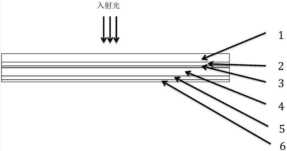
[0065] The first step is to prepare a P-type thin film crystalline silicon layer on the transparent conductive substrate of the AZO transparent oxide conductive layer based on glass:

[0066] (1.1) Preparation of P-type α-Si:H amorphous silicon thin film: Place the transparent conductive substrate of AZO based on glass on the sample stage of PECVD equipment, and use the PECVD method at a reaction pressure of 5Pa, a substrate temperature of 50°C, SiH 4 The gas flow rate is 0.lsccm, H 2 Gas flow rate is 1sccm, PH 3 Under the condition that the gas flow is 0.000lsccm, a 20nm thick P-type α-Si:H amorphous silicon film is grown on the transparent conductive substrate of the AZO transparent oxide conductive layer based on glass,

[0067] (1.2) Dehydrogenation of P-type α-Si:H amorphous silicon thin film: in high-purity N 2 A...

Embodiment 2

[0088] A method for preparing a thin-film crystalline silicon perovskite heterojunction solar cell according to this embodiment, the steps are as follows:

[0089] The first step is to prepare a P-type thin film crystalline silicon layer on the transparent conductive substrate of the ITO transparent oxide conductive layer based on glass:

[0090] (1.1) Preparation of P-type α-Si:H amorphous silicon thin film: Place the transparent conductive substrate on the sample stage of PECVD equipment, and through the PECVD method, at a reaction pressure of 26Pa, a substrate temperature of 200°C, SiH 4 The gas flow rate is 5 sccm, H 2 Gas flow rate is 50sccm, PH 3 Under the condition that the gas flow is 0.5 sccm, a 1510nm thick P-type α-Si:H amorphous silicon film is grown on the transparent conductive substrate of the ITO transparent oxide conductive layer based on glass,

[0091] (1.2) Dehydrogenation of P-type α-Si:H amorphous silicon thin film: in high-purity N 2 The P-type α-Si:H...

Embodiment 3

[0112] A method for preparing a thin-film crystalline silicon perovskite heterojunction solar cell according to this embodiment, the steps are as follows:

[0113] The first step is to prepare a P-type thin film crystalline silicon layer on the transparent conductive substrate of the FTO transparent oxide conductive layer based on glass:

[0114] (1.1) Preparation of P-type α-Si:H amorphous silicon thin film: Place the transparent conductive substrate on the sample stage of PECVD equipment, and through PECVD method, under the reaction pressure of 50Pa, substrate temperature of 350℃, SiH 4 Gas flow rate is 10sccm, H 2 Gas flow is l00sccm, PH 3 Under the condition that the gas flow is 1 sccm, a 3000nm thick P-type α-Si:H amorphous silicon film is grown on the transparent conductive substrate of the FTO transparent oxide conductive layer based on glass,

[0115] (1.2) Dehydrogenation of P-type α-Si:H amorphous silicon thin film: in high-purity N 2 The P-type α-Si:H amorphous s...


PUM

PropertyMeasurementUnit
thicknessaaaaaaaaaa
thicknessaaaaaaaaaa
thicknessaaaaaaaaaa

Abstract

The invention provides a thin film crystalline silicon perovskite heterojunction solar cell and a preparation method thereof, relates to a semiconductor device for converting optical energy to electric energy, and particularly provides a thin film crystalline silicon perovskite heterojunction solar cell having an electronic cavity composite suppression structure layer. The solar cell includes a transparent conductive substrate, a P-type thin film crystalline silicon layer, an electronic cavity composite suppression structure layer, a perovskite light absorption layer, an electronic transmission layer formed by compact titanium dioxide, and a back electrode. The perovskite light absorption layer and the P-type thin film crystalline silicon layer have matched energy levels, and the electronic cavity composite suppression structure layer formed by SiO2 is added between the P-type thin film crystalline silicon layer and the perovskite light absorption layer. The solar cell provided overcomes the defects of current leakage and internal short circuit of a thin film crystalline silicon perovskite heterojunction solar cell in the prior art.

Description

technical field [0001] The technical solution of the invention relates to a semiconductor device specially suitable for converting light energy into electric energy, specifically a thin-film crystal silicon perovskite heterojunction solar cell and a preparation method thereof. Background technique [0002] The thin-film crystalline silicon perovskite composite solar cell composed of thin-film crystalline silicon and perovskite not only overcomes the problems of insufficient stability and high preparation cost of ordinary perovskite solar cells due to the use of organic hole transport materials, but also overcomes the It overcomes the disadvantage of large amount of silicon material used in perovskite solar cells using bulk crystalline silicon as the hole transport material, and at the same time overcomes the disadvantage of amorphous silicon in perovskite solar cells using non-thin-film crystalline silicon as the hole transport material. Many material defects lead to perform...

Claims


Application Information

Patent Timeline
Patent Type & Authority Applications(China)
IPC IPC(8): H01L51/42H01L51/48
CPCH10K71/164H10K30/30Y02E10/549Y02P70/50H10K30/10H10K30/50
Inventor 田汉民毕文刚张天花中秋戎小莹杨瑞霞王伟
Owner HEBEI UNIV OF TECH
Why Eureka
Try Eureka