Chip packaging method

A packaging method and chip technology, which are applied in the field of micro-total analysis systems, can solve the problems of air bubbles on the bonding surface, chip products need vacuum packaging, and the bonding surface is not strong, and achieve high packaging strength, high fidelity, and simple packaging process. Effect

Inactive Publication Date: 2016-04-06
CAPITALBIO CORP
View PDF16 Cites 9 Cited by
  • Summary
  • Abstract
  • Description
  • Claims
  • Application Information

AI Technical Summary

Problems solved by technology

[0008] The purpose of the present invention is to provide a method for encapsulating microfluidic chips and finished products based on solid double-sided adhesive or single-sided adhesive. , which not only solves the problem of weak bonding surface and air bubbles in the conventional pressure bonding method, but also simultaneously solves the problem that chip products need vacuum packaging for long-term storage

Method used


Image

  • Chip packaging method
  • Chip packaging method
  • Chip packaging method

Examples


Embodiment 1

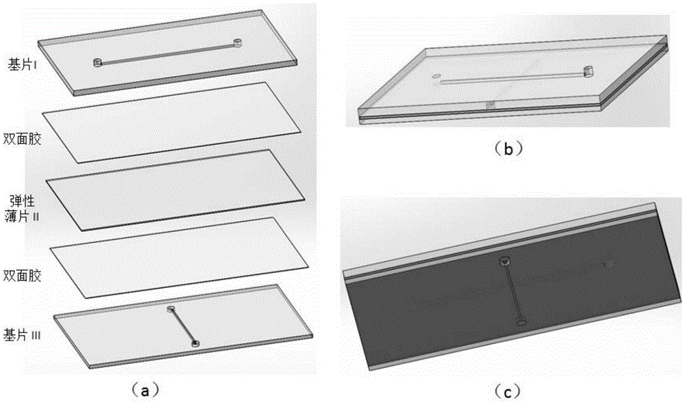
[0039] image 3 It is a schematic diagram of encapsulation of multi-layer sheets in the encapsulation method of the present invention.

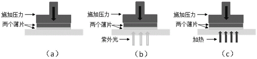
[0040] According to the procedure of the present invention, the lower surface of the microfluidic chip substrate I and the upper surface of the substrate III are cut as follows with a milling cutter image 3 The microstructure shown; use a perforator to punch through the holes corresponding to the inlet and outlet holes of the microstructure in the substrate I and the substrate III; seal the microstructures of the substrate I and the substrate III with the elastic sheet II covered with double-sided adhesive on both sides. Pipes and micropores; put the bonded chip into a packaging bag for vacuum packaging, and then place the bag on a pneumatic punching machine to punch the chip in the bag for 1 minute, so that the three layers of sheets are tightly bonded.

[0041] image 3 (a) is an exploded schematic diagram of a multilayer chip applying t...

Embodiment 2

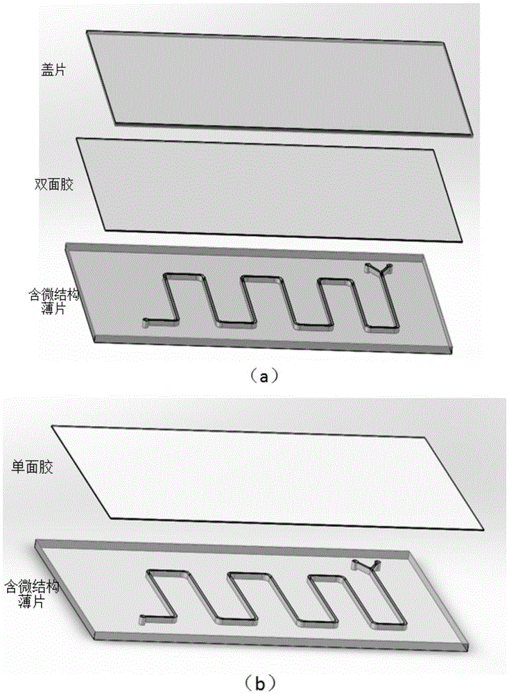
[0043] Such as Figure 4 As shown, the base and cover sheets can be of various shapes. First, attach the double-sided adhesive to the lower surface of the cover sheet, then attach the cover sheet covered with double-sided adhesive to the microstructure surface of the substrate, and then put the attached chip into the packaging bag for vacuum treatment. Finally, the packaging bag containing the chip was placed on the punching device for punching with a pressure of 0.7 MPa and kept for 1 minute so that the substrate and cover sheet of the microfluidic chip were tightly bonded. Figure 4 (a) is to add the solution centrifugation that contains dye to the chip after sealing, 70 ℃ heat 60 minutes chip physical picture, can observe that according to the chip that packaging process of the present invention makes even if long-term high-temperature heating, its adhesive surface There are no bubbles, and the microchannel is tightly sealed without leakage, which not only realizes the aes...


PUM


Abstract

The invention discloses a chip packaging method. In the method, one-step vacuum-pumping pressurization packaging is performed after a substrate and a cover plate of a micro-fluidic chip are laminated with a double-sided adhesive or a single-sided adhesive. Through adoption of the method, the problems of poor firmness of a bonding surface and remaining of a large quantity of blisters on the surface of the chip after bonding in a conventional solid-state double-sided adhesive bonding method are solved; the problems of micro-channel distortion and micro-channel blockage in a current micro-fluidic chip bonding process are solved; and an outer packaging procedure of a finished chip is implemented synchronously. The chip packaging method is simple and effective in auxiliary equipment and manufacturing process, and high fidelity of a chip micro-channel and high packaging strength of a packaged chip are ensured. A packaging procedure provided by the invention is particularly suitable for the field of manufacturing of micro-fluidic chips on a large scale at low cost.

Description

technical field [0001] The invention belongs to the technical field of Micro Total Analysis System (μ-TAS: Micro Total Analysis System), and relates to a chip packaging method. Background technique [0002] The microfluidic chip is made of microchannels, micropumps, microvalves, microreservoirs and other functional units on a substrate of several square centimeters through micromachining, precision injection molding, traditional mechanical processing and other technologies to realize the collection of microfluidics. A fast, efficient and low-consumption miniature full analysis system integrating sample preparation, sample injection, reaction, separation and detection. [0003] Microfluidic chip processing materials include various glass, metal, silicon wafers, polymer materials, etc. Polymer materials such as polydimethylsiloxane (PDMS), polymethyl methacrylate (PMMA), polycarbonate (PC) and various other plastics due to the advantages of cheap price, easy forming and low m...

Claims


Application Information

Patent Timeline
Patent Type & Authority Applications(China)
IPC IPC(8): B81C3/00
CPCB81C3/001B01L3/502707B01L2300/0803B01L2300/0816B01L2300/0887B81B7/0061B81B2201/058B01L2200/12
Inventor 王磊周鑫颖马丽林明仙冯金海
Owner CAPITALBIO CORP
Why Eureka
Try Eureka