Preparation method of cadmium selenide or cadmium sulfide two-dimensional monocrystal nanosheet

A single crystal nanometer, cadmium sulfide technology, applied in chemical instruments and methods, single crystal growth, single crystal growth and other directions, can solve the problems of restricting the application of nanometer optoelectronic devices, low crystallinity of nanosheets, and difficult solvent cleaning, etc. R&D and application, easy to make and apply, highly reproducible effect

Active Publication Date: 2016-04-06
TECHNICAL INST OF PHYSICS & CHEMISTRY - CHINESE ACAD OF SCI
View PDF5 Cites 36 Cited by
  • Summary
  • Abstract
  • Description
  • Claims
  • Application Information

AI Technical Summary

Problems solved by technology

However, some rare two-dimensional nanoplatelets based on these two materials are prepared by the liquid phase method (S.Ithurria, M.D.Tessier, B.Mahler, R.P.S.M.Lobo, B.DubertretandAl.L.Efros.Colloidalnanoplateletswithtwo-dimensionalelectronicstructure .NatureMaterials.2011,10,936–941.), the nanosheets prepared by this method have disadvantages such as low crystallinity, small size, and difficult cleaning by solvents, which greatly restrict their application in nano-optoelectronic devices

Method used


Image

  • Preparation method of cadmium selenide or cadmium sulfide two-dimensional monocrystal nanosheet
  • Preparation method of cadmium selenide or cadmium sulfide two-dimensional monocrystal nanosheet
  • Preparation method of cadmium selenide or cadmium sulfide two-dimensional monocrystal nanosheet

Examples


Embodiment 1

[0042] (1) Preparation of mica sheet substrate:

[0043] 1. Use scissors to divide the mica sheet into rectangles with a size of 2cm*3cm.

[0044] 2. Use the sharp tweezers at the top to dissociate the mica sheet into two thin sheets naturally from the middle, and use the new dissociated surface as the growth substrate.

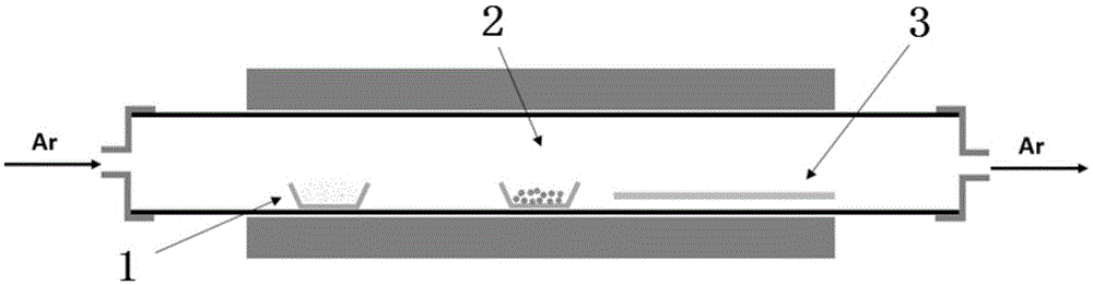
[0045] (2) Weigh 0.1 gram of CdCl 2 powder, which is then placed in the heated central area of ​​a tube furnace. Weigh 0.79 g of Se powder and place it in the ceramic tube about 20 cm upstream from the heating center, and place the mica substrate on the downstream of the heating center of the single-temperature zone tube furnace, about 5-20 cm away from the center.

[0046] (3) Turn on the mechanical pump to evacuate, and when the pressure in the furnace drops to 0.1Pa, quickly fill in high-purity argon to bring the pressure in the chamber back to atmospheric pressure.

[0047] (4) Rapidly raise the temperature to 750° C. at a speed of 20° C. / min and keep ...

Embodiment 2

[0056] (1) Preparation of mica sheet substrate:

[0057] 1. Use scissors to divide the mica sheet into rectangles with a size of 2cm*3cm.

[0058] 2. Use the sharp tweezers at the top to dissociate the mica sheet into two thin sheets naturally from the middle, and use the new dissociated surface as the growth substrate.

[0059] (2) Weigh 0.1 gram of CdCl 2 powder, which is then placed in the heated central area of ​​a tube furnace. Weigh 0.32 g of S powder and place it in the ceramic tube about 24 cm upstream from the heating center, and place the mica sheet substrate downstream of the heating center of the single-temperature zone tube furnace, about 5-20 cm away from the center.

[0060] (3) Turn on the mechanical pump to evacuate, and when the pressure in the furnace drops to 0.1Pa, quickly fill in high-purity argon to bring the pressure in the chamber back to atmospheric pressure.

[0061] (4) Rapidly raise the temperature to 750° C. at a speed of 20° C. / min and keep it f...

Embodiment 3

[0069] (1) Preparation of mica sheet substrate:

[0070] 1. Use scissors to divide the mica sheet into rectangles with a size of 2cm*3cm.

[0071] 2. Cleavage the mica sheet into two sheets naturally from the middle with the tipped tweezers, and use the new cleavage plane as the growth substrate.

[0072] (2) Weigh 0.1 gram of CdCl 2 powder, which is then placed in the heated central area of ​​a tube furnace. Weigh 0.79 g of selenium powder and place it in the ceramic tube about 26 cm upstream from the heating center, and place the mica sheet substrate sequentially on the downstream of the heating center of the single temperature zone tube furnace, about 5-20 cm away from the center.

[0073] (3) Turn on the mechanical pump to evacuate, and when the pressure in the furnace drops to 0.1Pa, quickly fill in high-purity argon to bring the pressure in the chamber back to atmospheric pressure.

[0074] (4) Rapidly raise the temperature to 800° C. at a speed of 30° C. / min and keep...


PUM

PropertyMeasurementUnit
band gapaaaaaaaaaa
band gapaaaaaaaaaa

Abstract

The invention discloses a preparation method of a cadmium selenide or cadmium sulfide two-dimensional monocrystal nanosheet. The method comprises the steps that the CdSe or CdS two-dimensional monocrystal nanosheet is prepared through a van der Waals epitaxial growth technology, the method is characterized in that a mica sheet which is smooth in surface and free of chemical dangling bond is adopted to serve as a substrate, CdCl2 powder or Se powder or S powder serves as a source material, argon serves as carrier gas, CdCl2 stream is reacted with Se or S steam to form CdSe or CdS steam at high temperature, and the steam is deposited on the mica sheet for nucleation and epitaxially grows into the CdSe or CdS two-dimensional monocrystal nanosheet. The preparation method of the cadmium selenide or cadmium sulfide two-dimensional monocrystal nanosheet is easy to operate, low in cost and strong in controllability, the obtained CdSe or CdS has the advantages of being good in size uniformity, high in degree of crystallinity and the like, and important research value and wide application prospect in the fields of solar cells, field effect transistors, photoelectric detectors, photocatalyses and the like are achieved.

Description

technical field [0001] The invention relates to the field of nanometer semiconductor technology. More specifically, it relates to a method for preparing large-area two-dimensional single-crystal nanosheets of cadmium selenide (CdSe) and cadmium sulfide (CdS). Background technique [0002] In recent years, two-dimensional nanomaterials have aroused a worldwide research boom due to their unique structure and physical and chemical properties, and have shown great application potential in both basic research and industrial production. The most widely studied two-dimensional materials are mainly layered materials based on graphene and transition metal chalcogenides. Graphene has the advantages of high strength and high carrier mobility, but the intrinsic graphene band gap is zero, resulting in low current switching efficiency of field effect transistors based on it. Layered transition metal chalcogenides are similar in structure to graphene, and the weaker van der Waals interac...

Claims


Application Information

Patent Timeline
Patent Type & Authority Applications(China)
IPC IPC(8): C30B29/48C30B29/50C30B29/64C30B25/18
CPCC30B25/18C30B29/48C30B29/50C30B29/64
Inventor 孟祥敏朱丹丹夏静王磊李玄泽
Owner TECHNICAL INST OF PHYSICS & CHEMISTRY - CHINESE ACAD OF SCI
Why Eureka
Try Eureka