Semiconductor device based on double patterns and manufacturing method thereof and electronic device
A semiconductor and double-patterning technology, which is applied in semiconductor/solid-state device manufacturing, circuits, electrical components, etc., can solve problems such as performance degradation and affecting the performance of semiconductor devices, and achieve good uniformity and consistency, good uniformity and consistency , the effect of good craftsmanship
- Summary
- Abstract
- Description
- Claims
- Application Information
AI Technical Summary
Problems solved by technology
Method used
Image

Examples
Embodiment 1
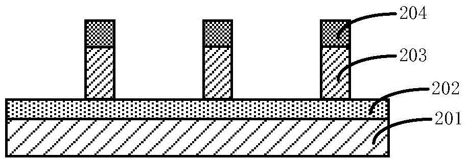
[0076] Attached below Figure 2a -2K further describes the method of the present invention, wherein Figure 2a -2K is a schematic diagram of the process of fabricating a semiconductor device based on a double-patterning method in an embodiment of the present invention.
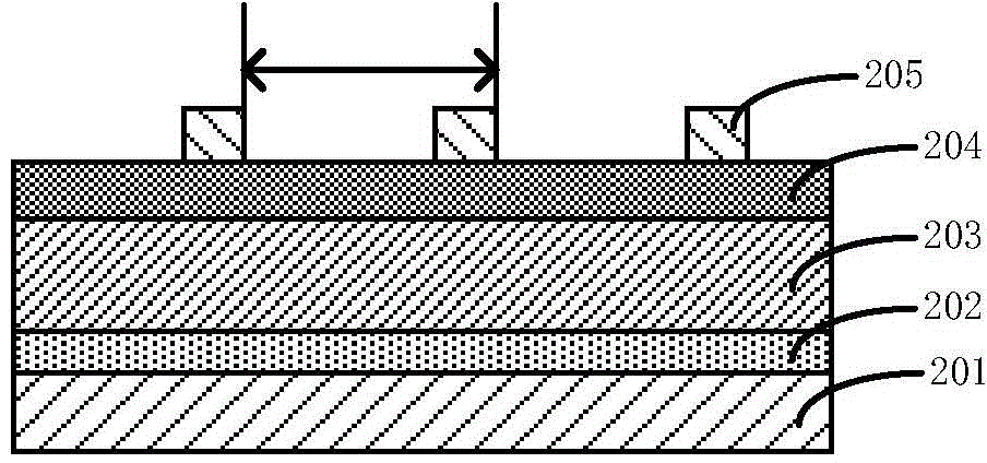
[0077] Step 201 is firstly performed, providing a semiconductor substrate 201 on which a dummy pattern material layer 203 , a hard mask material layer 204 and a patterned mask layer 205 are formed.
[0078] Specifically, such as Figure 2a As shown, the semiconductor substrate 201 may be at least one of the materials mentioned below: silicon, silicon-on-insulator (SOI), silicon-on-insulator (SSOI), silicon-germanium-on-insulator (S-SiGeOI ), silicon germanium on insulator (SiGeOI) and germanium on insulator (GeOI), etc.
[0079] Optionally, an isolation structure may also be formed in the semiconductor substrate, and the isolation structure is a shallow trench isolation (STI) structure or a local oxide of s...
Embodiment 2
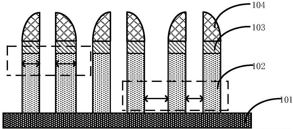
[0134] The present invention also provides another situation of semiconductor preparation, such as Figure 3a-3b As shown, the distance between the first spacers is M, and the distance between the second spacers is N. In this embodiment, the M>N, such as Figure 3a shown.
[0135] Then etch back the size of the second spacer to reduce the size of the second spacer so that the distances between the spacer arrays are equal
[0136] In this step, the distance between the first spacers and the distance between the second spacers are measured respectively, and then the method of wet stripping or etching trimming is used to reduce the first spacers or the second spacers. Dimensions of the spacer wall.
[0137] For the rest of the preparation steps, reference can be made to Example 1, which will not be repeated here.
Embodiment 3
[0139] The present invention also provides a semiconductor device, which is prepared by the method described in Embodiment 1 or 2. The pattern of the semiconductor device prepared by the method of the invention has good uniformity and consistency, so as to further improve the performance and yield of the semiconductor device.
PUM
 Abstract
Description
Claims
Application Information