

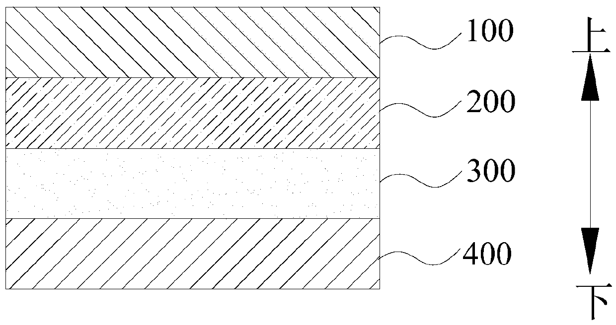
Solar cell and method for preparing solar cell
A technology of solar cells and electrodes, applied in circuits, photovoltaic power generation, electrical components, etc., can solve problems such as solar cells that need to be improved, and achieve the effect of improving performance
- Summary
- Abstract
- Description
- Claims
- Application Information
AI Technical Summary
Problems solved by technology
Method used
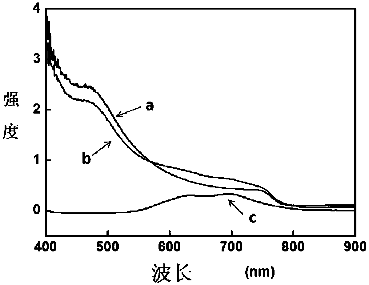
Image

Examples
Embodiment 1
[0121] The first step is to prepare and clean the transparent conductive electrode
[0122] On the glass substrate, the fluorine-doped tin oxide anode layer with a thickness of 120 nanometers is etched into the desired electrode pattern, and the etched FTO glass is sequentially washed with detergent, deionized water, absolute ethanol, acetone, and isopropanol. Ultrasonic for 15 minutes respectively, cleaned, placed in an oven, dried at 120°C, and treated with UV / ozone for 30 minutes.
[0123] The second step is to prepare the electron transport layer
[0124] The precursor solution of titanium diacetylacetonate diisopropoxide was coated on the surface of the transparent conductive electrode by scraping method, and then sintered at 450°C for 30min in a muffle furnace to form an electron transport layer with a thickness of 45nm.
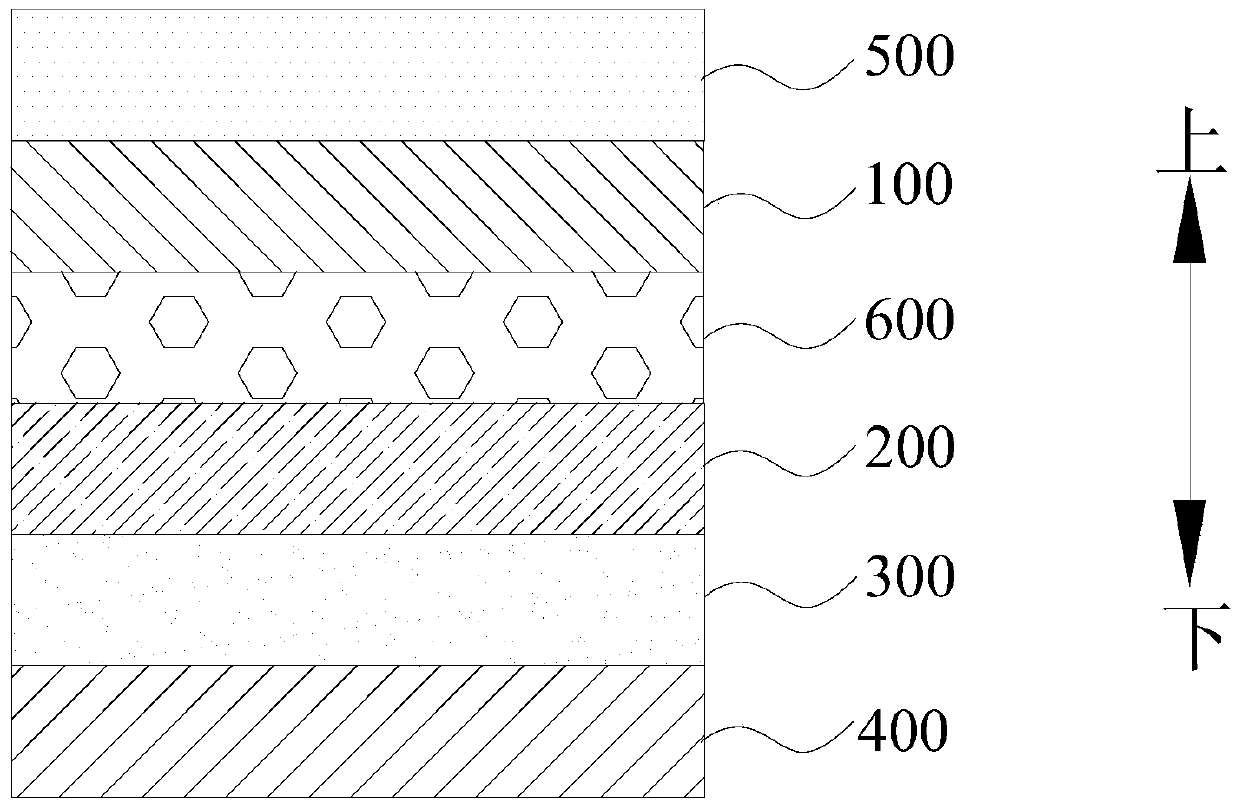
[0125] The third step is to prepare the mesoporous layer
[0126] The interface modification layer was prepared by spin coating on the surface of th...
Embodiment 2
[0139] The first step is to prepare and clean the transparent conductive electrode
[0140] On the glass substrate, etch the indium tin oxide anode layer with a thickness of 120 nanometers into the required electrode pattern, and place the etched ITO glass in detergent, deionized water, absolute ethanol, acetone, and isopropanol in sequence Sonicate them for 15 minutes, clean them, put them in an oven, dry them at 120°C, and treat them with UV / ozone for 30 minutes.
[0141] The second step is to prepare the electron transport layer
[0142] By evaporation method, the preparation of C 60 Thin film, the film thickness is 2 to 30nm, and the optimal thickness is 5nm.
[0143] electron transport layer
[0144] The third step and the fourth step are the same as the fourth step and the fifth step of Example 1.
[0145] The fifth step, preparing the counter electrode is the same as the sixth step of Example 1.
[0146] The device structure of the planar heterojunction perovskite ...
PUM
| Property | Measurement | Unit |
|---|---|---|
| Thickness | aaaaa | aaaaa |
| Thickness | aaaaa | aaaaa |
Abstract
Description
Claims
Application Information