Trench gate power MOSFET (Metal Oxide Semiconductor Field Effect Transistor) and manufacturing method thereof

A manufacturing method and trench gate technology are applied in the manufacture of trench gate power MOSFETs and in the field of trench gate power MOSFETs, which can solve the problems of increasing channel density, reducing on-resistance, poor channel turn-on voltage uniformity, etc. The effect of reducing pitch and increasing channel density

Active Publication Date: 2016-05-04
SHANGHAI HUAHONG GRACE SEMICON MFG CORP
View PDF4 Cites 6 Cited by
  • Summary
  • Abstract
  • Description
  • Claims
  • Application Information

AI Technical Summary

Problems solved by technology

[0005] In order to further increase the channel density and reduce the on-resistance (Rdon) of the device, the easiest way is to further reduce the cell size design; in the process of reducing the design size, the trench is further reduced due to equipment (cost) and gate formation process Factors such as increased difficulty have basically reached the limit, and simply reducing the cell size requires reducing the distance between the contact hole and the trench. The existing method will encounter failure of the gate-source short circuit device caused by insufficient registration accuracy between the contact hole and the gate trench. The channel doping concentration is greatly affected by contact hole implantation, resulting in poor channel turn-on voltage uniformity and other problems, which cannot be mass-produced
The specific description is as follows: in the prior art, the contact hole 109 is defined by a photolithography process, that is, the size and position of the contact hole 109 are defined by the photolithography process, and the gate trench and the gate lead-out trench are also defined by the photolithography process. Defined by the lithography process, due to the lithography process has a certain precision limit, the position and width of the contact hole 109, the gate trench and the gate lead-out trench have deviations within the precision range of the lithography process, this lithography process The deviation caused by the accuracy makes it necessary to consider the registration redundancy between the contact hole 109 and the trench at the bottom, such as the gate trench and the gate lead-out trench, when making the trench gate power transistor, the contact hole 109 and the trench The gap between the grooves must be large enough to prevent problems such as the drift of the threshold voltage, that is, the channel turn-on voltage caused by the offset of the exposure of the contact hole 109
This limits the possibility of reducing the on-resistance by increasing the channel density by shrinking the mesa size between the gate trenches
That is to say, the distance between the gate trenches in the prior art has a limit value related to the photolithography process, which cannot be further reduced, so that it is impossible to further increase the channel density by reducing the distance between the gate trenches so that Lower on-resistance

Method used


Image

  • Trench gate power MOSFET (Metal Oxide Semiconductor Field Effect Transistor) and manufacturing method thereof
  • Trench gate power MOSFET (Metal Oxide Semiconductor Field Effect Transistor) and manufacturing method thereof
  • Trench gate power MOSFET (Metal Oxide Semiconductor Field Effect Transistor) and manufacturing method thereof

Examples


Embodiment Construction

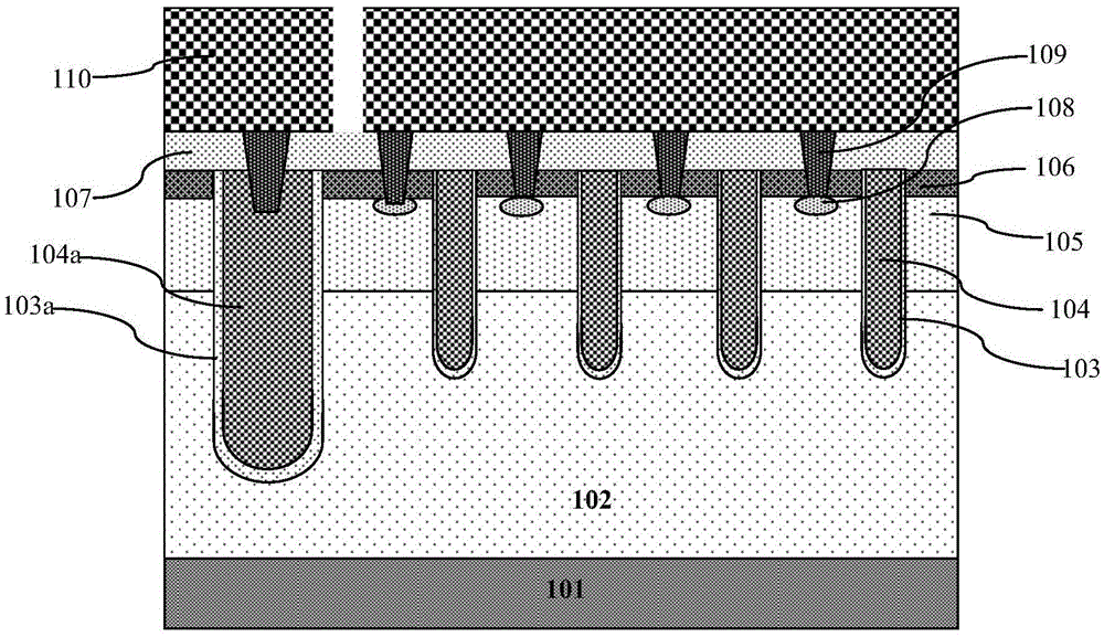
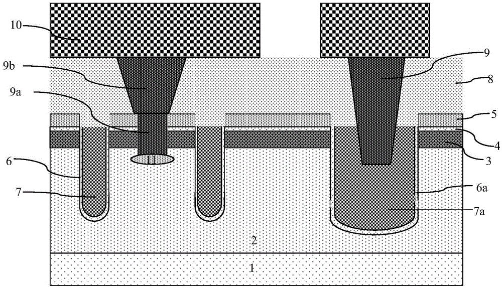
[0054] Such as figure 2 As shown, it is a schematic structural diagram of a trench gate power MOSFET according to an embodiment of the present invention; the trench gate power MOSFET according to an embodiment of the present invention includes:

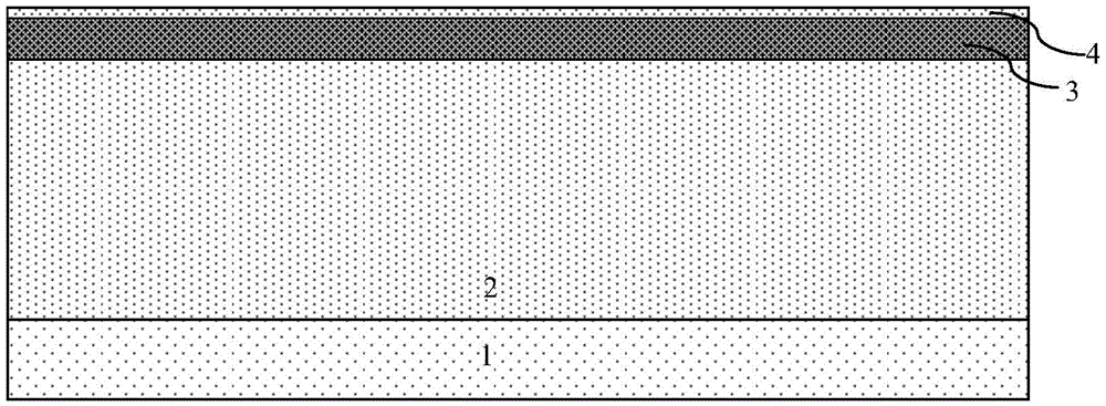
[0055] A semiconductor epitaxial layer 1, the semiconductor epitaxial layer 1 is formed on the surface of a semiconductor substrate. Preferably, the semiconductor substrate is a silicon substrate, and the semiconductor epitaxial layer 1 is a silicon epitaxial layer.

[0056] A hard mask layer formed by stacking the first silicon oxide layer 4 and the second silicon nitride layer 5 is formed on the surface of the semiconductor epitaxial layer 1, and a first trench is formed in the hard mask layer. The gate groove pattern and the source region contact hole pattern defined by the mask plate at the same time; the bottom region 9a with a plurality of gate trenches and a plurality of source region contact holes is formed in the semiconduc...


PUM


Abstract

The invention discloses a trench gate power MOSFET (Metal Oxide Semiconductor Field Effect Transistor), which comprises a semiconductor epitaxial layer, wherein a hard mask layer is formed on the surface of the semiconductor epitaxial layer; a gate trench pattern and a source area contact hole pattern which are simultaneously defined by a first trench mask plate are formed in the hard mask layer; the sizes of gate trenches are defined by the gate trench pattern; bottom areas of source area contact holes are completely defined by the source area contact hole pattern of the hard mask layer; a gate dielectric layer and a polysilicon gate are formed in each gate trench; an interlayer film is formed on the surface of the hard mask layer and the surface of the polysilicon gate; top areas of the source area contact holes penetrate through the interlayer film and are defined by a contact hole mask plate; the source area contact holes are formed by self-aligned superposition of the top areas and the bottom areas; and structures without registration deviation are formed between the top areas of the source area contact holes and the gate trenches. The invention also discloses a manufacturing method of the trench gate power MOSFET. According to the trench gate power MOSFET and the manufacturing method thereof, a distance between the gate trenches can be reduced and the channel density is increased.

Description

technical field [0001] The invention relates to the field of manufacturing semiconductor integrated circuits, in particular to a trench gate power MOSFET; the invention also relates to a manufacturing method of the trench gate power MOSFET. Background technique [0002] In semiconductor integrated circuits, the structure of a common trench power MOS transistor with a small cell size is as follows: figure 1 As shown, this structure is generally used in 1.0 micron to 1.8 micron cell size designs. A semiconductor epitaxial layer such as a silicon epitaxial layer 102 is formed on a semiconductor substrate such as a silicon substrate 101, and a body region (body) 105 and a source region 106 are sequentially formed on the surface of the semiconductor epitaxial layer 102; in the semiconductor epitaxial layer 102 A plurality of gate trenches are formed, and a gate dielectric layer such as a gate oxide layer 103 is formed on the bottom surface and sides of the gate trenches, and the...

Claims


Application Information

Patent Timeline
Patent Type & Authority Applications(China)
IPC IPC(8): H01L21/336H01L21/28H01L29/423H01L29/78
CPCH01L29/401H01L29/4236H01L29/42364H01L29/66666H01L29/78
Inventor 邵向荣
Owner SHANGHAI HUAHONG GRACE SEMICON MFG CORP
Why Eureka
Try Eureka