Method for preparing memristor based on nanoscale single layer Bi (1-x) CaxFeO3-x/2 resistance variable film

A memristor, nanoscale technology, applied in the field of nonlinear circuit applications, can solve the problems of long preparation period, complex preparation process, and few memristor models, and achieves easy physical realization, simple preparation process, and low control difficulty. Effect

Active Publication Date: 2016-05-04
SHANDONG UNIV OF SCI & TECH
View PDF5 Cites 0 Cited by
  • Summary
  • Abstract
  • Description
  • Claims
  • Application Information

AI Technical Summary

Problems solved by technology

[0005] (1) In recent years, new memristor materials and memristor systems have been continuously reported, but there are still few physically realized memristor models, and they are relatively single, and there is no unified universal model to describe the behavior of memristors
[0006] Most of the physical memristors reported in recent years are proposed for a certain type of application or to simulate a certain function (such as high-density non-volatile memory, CrossbarLatch technology, simulated synapse), and most of them use HP memristors. The switch model and working mechanism, and the manufacturing process is complicated and the cost is high. It is not general and universal for the study of memristor characteristics, memristor circuit theory and electronic circuit design.
[0007] (2) Commercial production has not yet been realized
[0008] It is difficult for most researchers to obtain a real memristor element, so many researchers cannot carry out hardware experiments in the real physical sense due to the lack of memristor elements when studying memristors and memristor circuits. Rely on simulation or simulated circuits for experimental research
However, the memristor simulation model and the analog circuit are far from the actual memristor characteristics, and the hardware implementation using the analog circuit is more concerned with simulating the memristor mathematical model and ignoring the essential physical characteristics of the memristor
[0009] (3) The preparation of physical memristors that have been reported requires high requirements and harsh conditions in terms of raw material selection and preparation process methods, and it is difficult for laboratories or scientific research units with ordinary conditions to complete the preparation of related physical memristor components.
[0016] 2. The preparation process is complicated, the preparation cycle is long, and the energy consumption is high:
[0018] In addition, it also has the problems and deficiencies of relatively harsh process conditions and low product rate.

Method used


Image

  • Method for preparing memristor based on nanoscale single layer Bi (1-x) CaxFeO3-x/2 resistance variable film
  • Method for preparing memristor based on nanoscale single layer Bi (1-x) CaxFeO3-x/2 resistance variable film
  • Method for preparing memristor based on nanoscale single layer Bi (1-x) CaxFeO3-x/2 resistance variable film

Examples


Embodiment 1

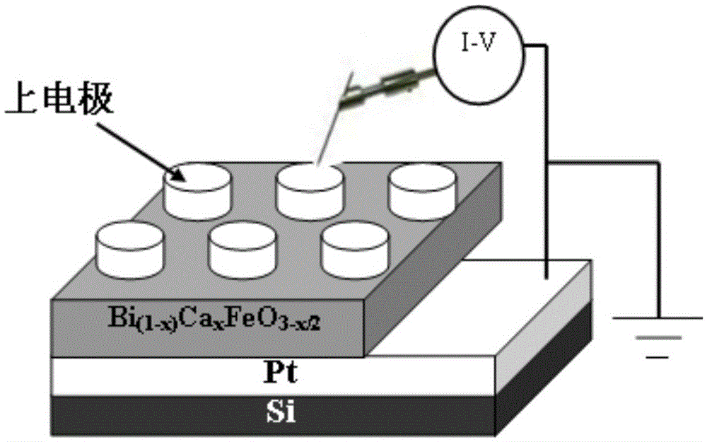
[0095] The preparation method of memristor all comprises the following steps:

[0096] The first step, prepare Bi (1-x) Ca x FeO 3-x / 2 target, the specific steps are as follows:

[0097] (1), raw material mixing:

[0098] Bi(NO 3 ) 3 ·5H 2 o 3 : Ca(NO 3 ) 2 4H 2 o 3 : Fe(NO 3 ) 3 9H 2 o 3 =99:1:100 (molar ratio) mixed;

[0099] Dissolve the above mixture in 10%-20% dilute nitric acid, place it on a magnetic stirrer, and stir to make it completely dissolve;

[0100] (2), powder preparation

[0101] Slowly add NaOH solution dropwise to the above solution until the precipitation is complete, filter the precipitate and wash it with deionized water, add NaOH solution dropwise and adjust the pH value, put it into a reaction kettle, and put it in a constant temperature drying box that has reached a predetermined temperature of 200°C in advance , hydrothermal reaction for 24 hours;

[0102] After the hydrothermal reaction, the reactor was naturally cooled to room te...
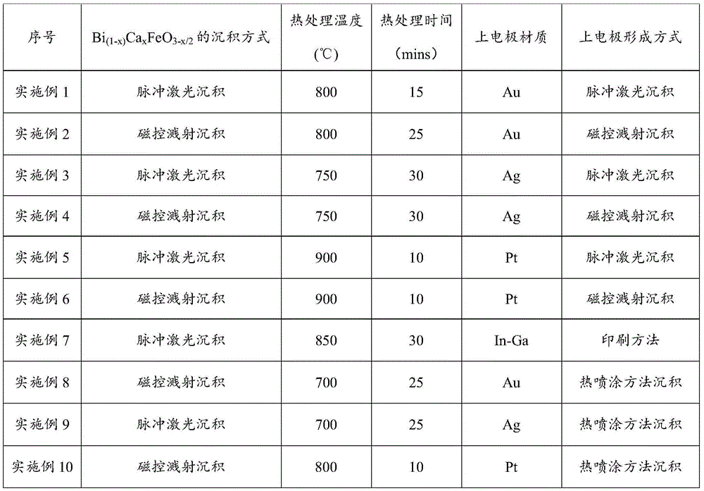
Embodiment 2

[0115] In addition to preparing Bi (1-x) Ca x FeO 3-x / 2 The raw material formula of the target is:

[0116] Bi(NO 3 ) 3 ·5H 2 o 3 : Ca(NO 3 ) 2 4H 2 o 3 : Fe(NO 3 ) 3 9H 2 o 3 =98: 2: 100 (molar ratio) and each parameter in the following table 1;

[0117] All the other are the same as in Example 1.

Embodiment 3

[0119] In addition to preparing Bi (1-x) Ca x FeO 3-x / 2 The raw material formula of the target is:

[0120] Bi(NO 3 ) 3 ·5H 2 o 3 : Ca(NO 3 ) 2 4H 2 o 3 : Fe(NO 3 ) 3 9H 2 o 3 =97: 3: 100 (molar ratio) and each parameter in the following table 1;

[0121] All the other are the same as in Example 1.


PUM

PropertyMeasurementUnit
Diameteraaaaaaaaaa
Thicknessaaaaaaaaaa
Thicknessaaaaaaaaaa

Abstract

The invention discloses a method for preparing a memristor based on a nanoscale single layer Bi (1-x) CaxFeO3-x / 2 resistance variable film. The method applies a principle of taking a hole and an ionized oxygen ion generated by the resistance variable film under a bias voltage as carriers, and depending on the change of an output of the resistance variable film to realize the resistance variation of a device, and on the basis of the prior art, the method begins from two aspects of simplifying the technology and improving a material formula of the resistance variable film: a step of pre-sintering a ceramic material of the resistance variable film is omitted, and a raw material with a higher metal ion valence and a lower ceramic sintering temperature is selected, and a lower calcination temperature is adopted, so that a Ca 2+ part can perform A-site substitution on a Bi 3+ part, so as to increase the lattice defect and hole inside the resistance variable film, and increase the asymmetry of a molecular structure of a resistance variable film layer; therefore, the above technical means simplify the preparation technology, improve the production efficiency, and reduce the production energy consumption and the production cost; meanwhile, the memristive performance and yield of the memristor can be greatly improved.

Description

technical field [0001] The invention relates to a method for preparing a memristor, in particular to a method based on nanoscale single-layer Bi (1-x) Ca x FeO 3-x / 2 The invention discloses a preparation method of a resistive variable film memristor; it belongs to the application field of nonlinear circuits. Background technique [0002] Memristors, also known as memristors, are the fourth passive circuit element after resistors, capacitors, and inductors. Due to its non-volatile, synaptic function and nanoscale structure, it is widely used in high-density non-volatile memory, artificial neural network, large-scale integrated circuit, reconfigurable logic and programmable logic, bioengineering, pattern recognition, signal Processing and other fields have great application prospects. And it is expected to pave the way for the development of non-volatile storage devices with unlimited storage precision and ultra-high storage density, artificial neural networks capable of a...

Claims


Application Information

Patent Timeline
IPC IPC(8): H01L45/00C23C14/35B82Y10/00
CPCC23C14/35B82Y10/00H10N70/00
Inventor 李玉霞窦刚郭梅于洋李煜孙钊
Owner SHANDONG UNIV OF SCI & TECH
Why Eureka
Try Eureka