Method based on 3D printing for manufacturing LED devices

An LED device, 3D printing technology, applied in semiconductor devices, circuits, electrical components, etc., can solve the problems of complex electrode formation process, photoresist pollution, epitaxial wafer ion damage, etc., to reduce lithography and etching steps, Fast molding speed, reducing the effect of photolithography and etching process steps

Active Publication Date: 2016-05-11
TAIYUAN UNIV OF TECH
View PDF5 Cites 9 Cited by
  • Summary
  • Abstract
  • Description
  • Claims
  • Application Information

AI Technical Summary

Problems solved by technology

Not only that, the electrode formation process is not only complicated, but also needs to replace multiple sets of masks, multiple photolithography, multiple wet and dry etching processes, such as figure 1 As shown, it is also easy to cause ion damage and photoresist pollution to the epitaxial wafer

Method used


Image

  • Method based on 3D printing for manufacturing LED devices
  • Method based on 3D printing for manufacturing LED devices
  • Method based on 3D printing for manufacturing LED devices

Examples


Embodiment Construction

[0024] In order to make the purpose, technical solution and advantages of the present invention clearer, the present invention will be further described below in conjunction with the accompanying drawings.

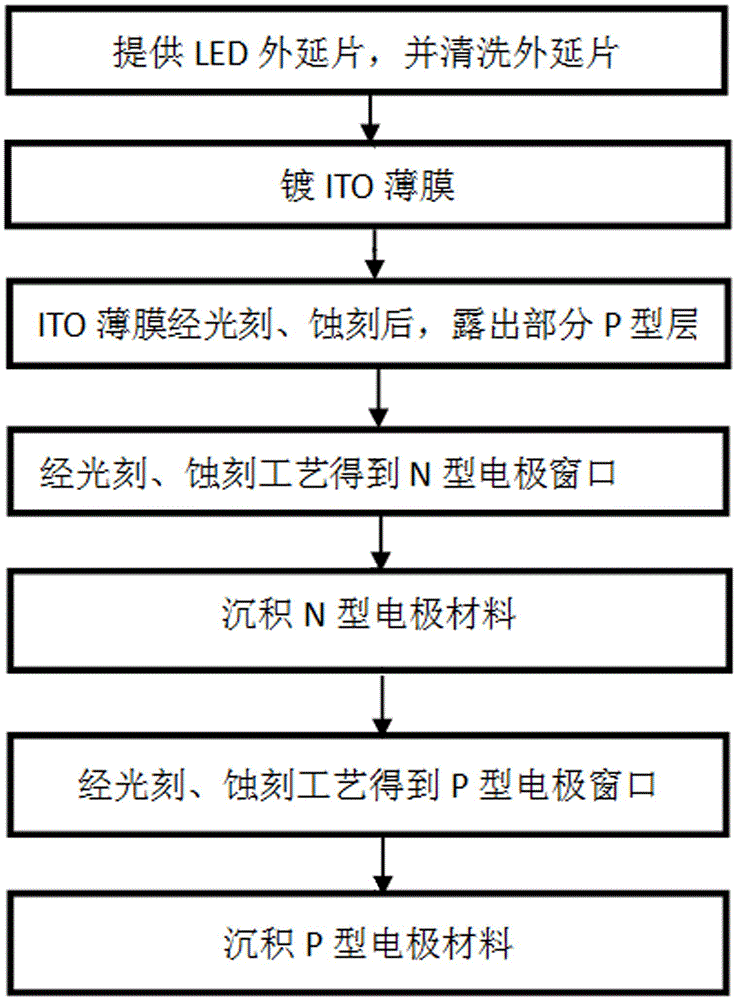
[0025] figure 1 It is the flow chart of traditional LED device electrode production. As shown in the figure, forming electrodes on epitaxial wafers requires multi-step photolithography and etching processes such as etching ITO film, etching n-type layer electrode window and p-type layer electrode window.

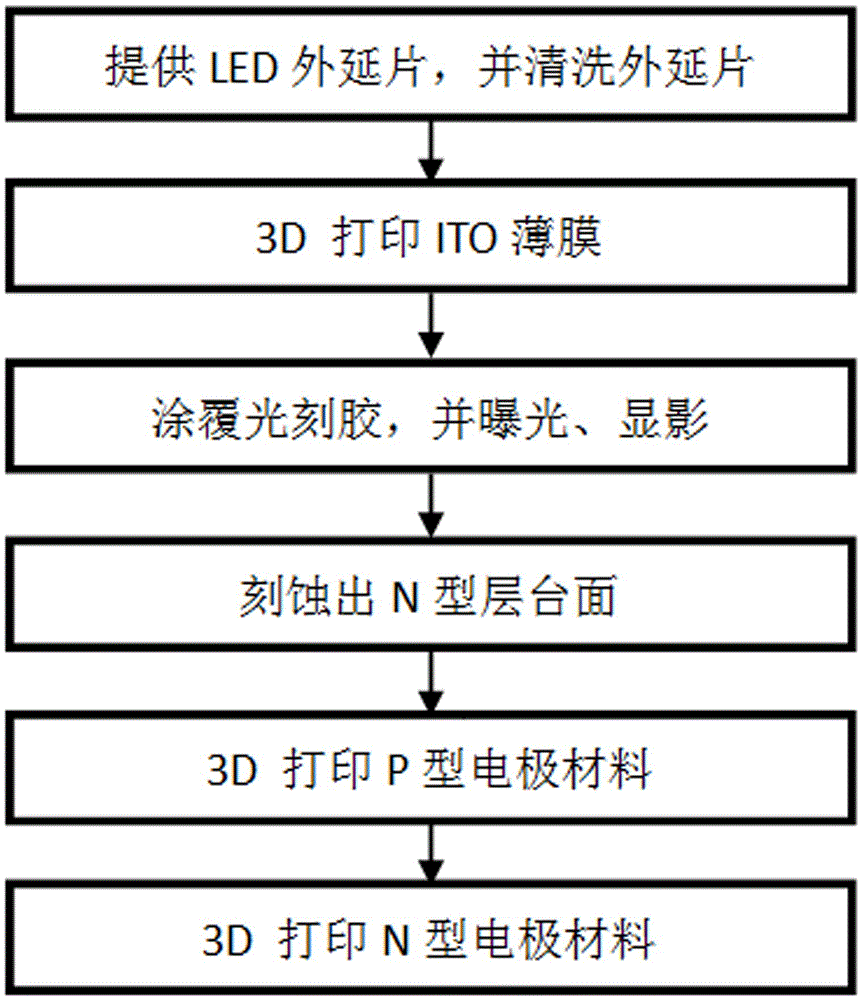
[0026] figure 2 The flow chart for making LED device electrodes based on 3D printing, as shown in the figure, to form electrodes on the epitaxial wafer, only one etching process is required to etch the epitaxial wafer to expose the n-type mesa, which greatly simplifies the process of LED device electrodes Process, shorten the production cycle. It can also reduce the probability of photoresist contamination and ion damage to the epitaxial wafer during the photolithogra...


PUM


Abstract

The invention belongs to the photoelectron device field and particularly relates to a method based on 3D printing for manufacturing LED devices. According to the method, epitaxial wafer which at least has a buffer layer, an N-type layer, a multi-period quantum well active layer and a P-type layer and is generated by MOCVD or MBE is taken as a substrate material, an ITO conduction layer is printed on a P-type layer table top through 3D printing, an N-type layer table top is then etched, and N-type electrode and P-type electrode layers are then printed. The LED device electrode structure is formed through 3D printing, steps of photoetching and corrosion in an electrode manufacturing process can not only be reduced, the production period is shortened, pollution and damage to the epitaxial wafer in a photoetching and corrosion process can be reduced, damage of a high temperature annealing process during electrode formation to the quantum well active region interface structure can be reduced, and thereby light emitting efficiency of the LED devices can be improved.

Description

technical field [0001] The invention belongs to the field of optoelectronic devices, in particular to a method for preparing electrodes of LED devices based on 3D printing. Background technique [0002] Light Emitting Diode (Light Emitting Diode, LED) has the characteristics of high brightness, low energy consumption, long life, fast response and environmental protection, etc. fields. [0003] Most LED device chips use metal-organic vapor deposition or molecular beam epitaxy to grow epitaxial wafers on sapphire substrates, then deposit indium tin oxide (ITO) transparent conductive layers, and etch out N-type layer mesas to form N-type electrodes. , and finally form a P-type electrode. Among them, the epitaxial wafer structure mainly includes a buffer layer, an N-type layer, a multi-period quantum well active layer and a P-type layer. The ITO transparent conductive film must have good conductive properties, transparency and reliability. Common P-type electrode materials a...

Claims


Application Information

Patent Timeline
Patent Type & Authority Applications(China)
IPC IPC(8): H01L33/36H01L33/00
CPCH01L33/005H01L33/36
Inventor 许并社朱亚丹卢太平赵广洲
Owner TAIYUAN UNIV OF TECH
Why Eureka
Try Eureka