Preparation method of bismuth-layered compound superlattice

A superlattice and compound technology, applied in the manufacture/processing of thermoelectric devices, electrical components, circuits, etc., can solve the problems of high cost, opacity, and unfavorable expansion research and application of superlattice devices

Active Publication Date: 2016-05-11
UNIV OF ELECTRONICS SCI & TECH OF CHINA
View PDF5 Cites 13 Cited by
  • Summary
  • Abstract
  • Description
  • Claims
  • Application Information

AI Technical Summary

Problems solved by technology

But the technology must first deposit In on the Si(111) surface 2 Se 3 The buffer layer can successfully realize the Bi 2 Se 3 /In 2 Se 3 Superlattice growth; in order to meet the needs of high-temperature cracking of metal-organic compounds and low-temperature growth of bismuth compounds at the same time, a specially designed MOCVD growth device must be used, and the

Method used


Image

  • Preparation method of bismuth-layered compound superlattice
  • Preparation method of bismuth-layered compound superlattice
  • Preparation method of bismuth-layered compound superlattice

Examples


Embodiment 1

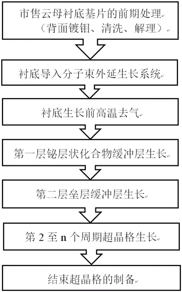
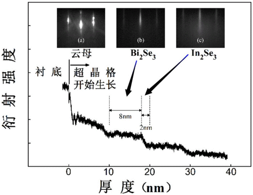
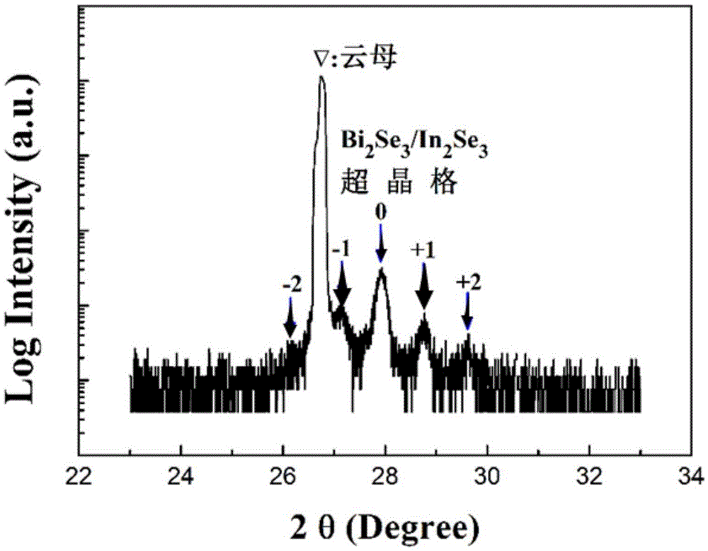
[0020] Embodiment 1: The periodic structure prepared on the muscovite substrate is Bi 2 Se 3 / In 2 Se 3 (8nm / 2nm) superlattice method is:

[0021]Step (1)——Using magnetron sputtering or electron beam evaporation to carry out molybdenum plating on the back of the muscovite sheet substrate; immerse the molybdenum-plated substrate in acetone and absolute ethanol solution in turn for ultrasonic cleaning, and The solution was washed for 3 minutes, and the cleaning was repeated 2 to 3 times; the surface of the muscovite was blown clean with high-purity nitrogen, and then the front side of the muscovite substrate was stuck on the tape, and then the tweezers were used to clamp the muscovite substrate along the direction perpendicular to the muscovite. The surface direction is quickly and evenly torn off to obtain the muscovite substrate;

[0022] Step (2)—Introduce the muscovite substrate into the molecular beam epitaxy system, heat it to 350-450°C to degas it, until the backgroun...

Embodiment 2

[0029] Example 2: The periodic structure prepared on the fluorine phlogopite substrate is Bi 2 Se 3 / In 2 Se 3 (8nm / 2nm) superlattice method is:

[0030] Step (1)—Using magnetron sputtering or electron beam evaporation to carry out molybdenum plating on the back of the fluorphlogopite sheet substrate; soak the molybdenum-plated substrate in acetone and absolute ethanol solutions for ultrasonic cleaning, and Wash in each solution for 3 minutes, and wash repeatedly 2 to 3 times; blow off the surface of fluorphlogopite with high-purity nitrogen, then stick the front side of the fluorphlogopite substrate on the tape, and then use tweezers to clamp the fluorphlogopite substrate along the Quickly and evenly tear it off perpendicular to the surface of fluorphlogopite to obtain a fluorphlogopite substrate;

[0031] Step (2)—Introduce the fluorine phlogopite substrate into the molecular beam epitaxy system, and heat it to 350-450°C to degas it until the background vacuum reaches 10...


PUM

PropertyMeasurementUnit
Thicknessaaaaaaaaaa
Thermal conductivityaaaaaaaaaa

Abstract

The invention relates to a preparation method of a bismuth-layered compound superlattice. According to the method, normal chemical cleaning is carried out on a mica substrate; the mica substrate is introduced into a vacuum system for heating and degassing after being split in atmosphere; and a superlattice film comprising a bismuth compound thin layer and a barrier material sequentially grows on the clean mica substrate. A bismuth compound layer is slowly deposited on the mica surface as a lattice mismatching buffer layer; a barrier material layer grows at the same temperature and speed to further improve the surface quality; and the bismuth compound layer and a barrier alternately grow under the conditions of keeping the growth temperature unchanged and improving the growth speed until growth within set superlattice periods is ended. The preparation method ensures that each material layer in the product superlattice grows in an ideal two-dimensional layered mode; and the technical effects that bismuth-layered compound superlattice quickly grows on the mica substrate, the superlattice interface is kept flat and the superlattice film with an adjustable period is obtained are achieved.

Description

technical field [0001] The invention relates to a method for preparing a bismuth layered compound superlattice. Background technique [0002] Bismuth layered compound (hereinafter referred to as bismuth compound) Bi 2 Se 3 with Bi 2 Te 3 It is not only a strong topological insulator (topological insulator is a newly discovered class of material morphology, their bulk electronic state is an insulator with energy gap, the surface is a metal state without energy gap, and these surface states are spin-polarized), and It is an excellent medium and low temperature thermoelectric conversion material. By ultra-thin Bi 2 Se 3 or Bi 2 Te 3 The superlattice structure composed of layers and other suitable barrier materials has been proved to have more novel topological quantum properties and greater thermoelectric conversion figure of merit than its bulk materials, such as Bi 2 Se 3 with Bi 2 Te 3 The formed superlattice thermoelectric figure of merit ZT≈2.4, much higher tha...

Claims


Application Information

Patent Timeline
IPC IPC(8): H01L35/00H01L35/34H01L35/16H01L35/18
CPCH10N10/853H10N10/00H10N10/852H10N10/01
Inventor 李含冬任武洋高磊张忠阳龙城佳李勇姬海宁戴丽萍周志华牛晓滨王志明
Owner UNIV OF ELECTRONICS SCI & TECH OF CHINA
Why Eureka
Try Eureka