Photon microflow detection chip based on LTCC integration

A detection chip and detector chip technology, applied in the field of micro-system sensing, can solve the problems of difficult control of micro-channel size, high cost, complex manufacturing technology, etc., achieve good anti-corrosion characteristics, reduce manufacturing cycle, and reduce manufacturing costs Effect

Active Publication Date: 2016-05-18
NO 54 INST OF CHINA ELECTRONICS SCI & TECH GRP
View PDF4 Cites 2 Cited by
  • Summary
  • Abstract
  • Description
  • Claims
  • Application Information

AI Technical Summary

Problems solved by technology

However, the thermodynamic properties of polymer materials are poor, which limits the use environment of fluidic chips, and its manufacturing technology is not easy to achieve one-time integrated manufacturing with electronic control units, and auxiliary processes such as bonding are required.
Inorganic materials such a

Method used


Image

  • Photon microflow detection chip based on LTCC integration
  • Photon microflow detection chip based on LTCC integration

Examples


example

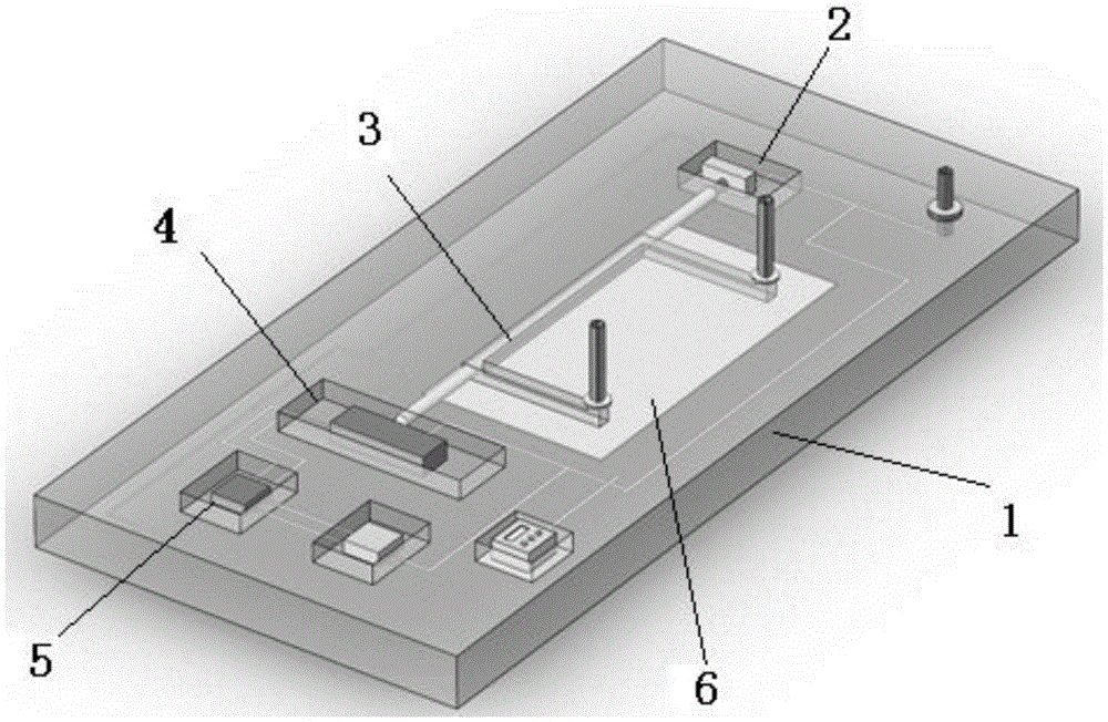
[0032] In the present invention, the LTCC substrate is made of Dupont951 ceramic sheet, and the thickness of each layer of the ceramic sheet is 114 μm. In this example, 20 layers of ceramic chips are used to construct the detection chip.

[0033] In the present invention, the optical fiber system uses the multimode bare optical fiber of Corning Corporation.

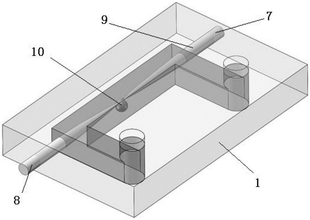
[0034] The schematic diagram of the photon sensing system in the microfluidic channel of the present invention is as follows: figure 2 shown. The cross-sectional size of the microfluidic channel is 1 mm × 1 mm. The photonic sensing system uses a high-Q optical microcavity sensing unit.

[0035] Based on the LTCC monolithic integrated photon microfluidic test method, the laser emitted by the light source chip is used as the signal source, and the photon detection source enters the photon sensing system in the microfluidic channel through the optical fiber system, and the detection of external substances is realized at ...


PUM


Abstract

The invention discloses a photon microflow detection chip based on LTCC integration, and belongs to the field of microsystem sensing detection. The chip integrates a micro light source, an optical fiber system, a photon sensing system, a detector chip, a signal processing chip and a temperature control board on an LTCC monolithic substrate, wherein a microflow channel and the optical fiber system are manufactured in the substrate, and therefore sensing of photons in the monolithic microflow system is achieved. The photon microflow detection chip has the advantages that integrated manufacturing of the optical fiber system and the photon sensing system can be more conveniently achieved in the LTCC substrate; parts such as the light source, the detector and the signal processor which are needed by the detection chip can be integrated on the LTCC substrate through a standard microassembly technology; controllable manufacturing of the microflow detection channel needed by the detection chip on the LTCC substrate can be conveniently achieved; LTCC has the good anti-corrosion characteristic and the high-temperature characteristic and can support the chip to be applied to a severe environment.

Description

technical field [0001] The invention belongs to the field of microsystem sensing, in particular to a photonic microflow detection chip realized on a low temperature co-fired ceramic (LTCC) substrate. technical background [0002] Optical detection method refers to the method of sensing external physical quantities by using photons as signal carriers in functional structures. Compared with traditional electronic signal sensing, it has the advantages of small transmission loss and strong anti-electromagnetic interference performance. Therefore, detection technologies based on photonic sensing have received extensive attention in both academia and industry. [0003] Microfluidic sensing chips can realize rapid sensing of substances on very small chips. The overall size of the chip is on the order of centimeters, and the fluid channel network inside the chip is on the order of micrometers. In sensing and detection applications, microfluidic sensing chips have the advantages o...

Claims


Application Information

Patent Timeline
IPC IPC(8): B01L3/00G01N21/17
CPCB01L3/5027B01L3/502707B01L2200/06B01L2200/143B01L2300/023B01L2300/0654B01L2300/0809G01N21/17
Inventor 严英占卢会湘唐小平党元兰赵飞李攀峰
Owner NO 54 INST OF CHINA ELECTRONICS SCI & TECH GRP
Why Eureka
Try Eureka