Gas source molecular beam epitaxy material growth method for component progressive transition layer

A technology of molecular beam epitaxy and growth method, which is applied in the field of semiconductor optoelectronic device preparation, can solve problems such as waste, long time interval, and slow switching, and achieve the effects of reducing transit time, reducing distortion, and improving device performance

Active Publication Date: 2016-05-25
湖南汇思光电科技有限公司
View PDF5 Cites 9 Cited by
  • Summary
  • Abstract
  • Description
  • Claims
  • Application Information

AI Technical Summary

Problems solved by technology

Even so, in the process of material growth using GSMBE technology, the number of switching between As and P should generally be reduced. This is because the switching between the two is relatively slow and the time interval is long, and the switching process is easy to generate dislocations and band steps at the interface. ; on the other hand, AsH 3 and PH 3 It is a highly toxic gas, the exhaust gas needs to be handled carefully, and the pumped part will also cause waste

Method used


Image

  • Gas source molecular beam epitaxy material growth method for component progressive transition layer
  • Gas source molecular beam epitaxy material growth method for component progressive transition layer
  • Gas source molecular beam epitaxy material growth method for component progressive transition layer

Examples


Embodiment 1

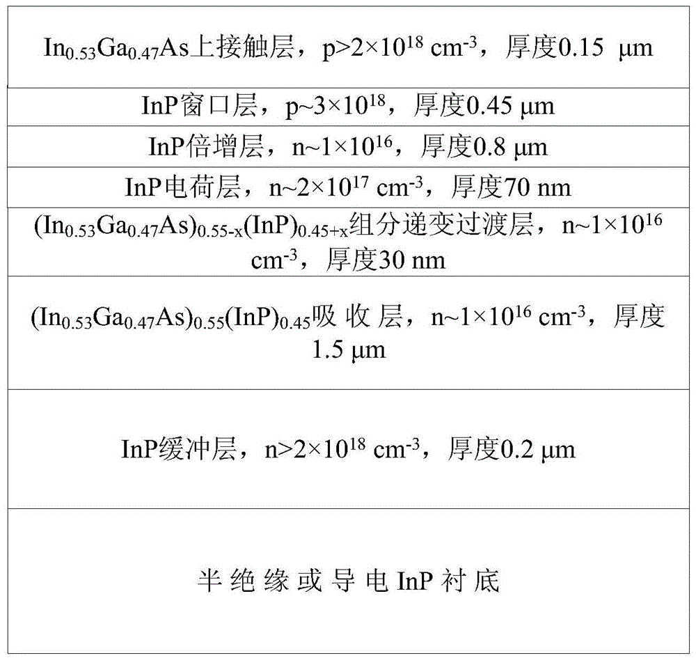
[0022] Growth of InGaAsP Avalanche Photodiode Structure Material with Cutoff Wavelength 1.25 μm on InP Substrate

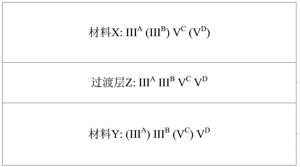
[0023] (1) need to grow (In 0.53 Ga 0.47 As) 0.55 (InP) 0.45 The avalanche photodiode epitaxial material adopts the separation of the absorption region charge region and the multiplication region, and has a transition layer (SAGCM) structure. The schematic diagram is as follows figure 2 As shown, that is: InP material is used as a buffer layer and is highly doped with Si (at the same time as the lower contact layer, n>2×10 18 cm -3 ), (In 0.53 Ga 0.47 As) 0.55 (InP) 0.45 The material is used as the absorbing layer for low doping Si or no doping (n~1×10 16 cm -3 ), undoped (In 0.53 Ga 0.47 As) 0.55-x (InP) 0.45+x The composition graded layer is used as the transition layer between the absorption layer and the charge layer, and the InP with low doping Si is used as the charge layer (n~2×10 17 cm -3 ), low-doped or undoped InP material as the multipl...

Embodiment 2

[0034] Growth of InGaAs Detector Structure Materials with Cutoff Wavelength of 2.6 Microns on InP Substrate

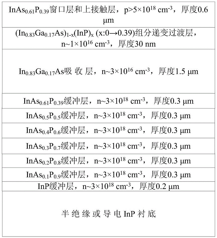
[0035] (1) The 50% cut-off wavelength at room temperature is required to be 2.6μmIn 0.83 Ga 0.17 Asp-i-n infrared photodetector structure epitaxial material, schematic diagram as shown image 3 As shown, before the formal growth, the beam source furnace temperature, substrate temperature and V group pressure values ​​when growing lattice-matched InP and InAsP buffer layers with different As and P compositions on the InP substrate were determined by preparatory growth. growing conditions.

[0036] (2) Using the gaseous source molecular beam epitaxy method, the semi-insulating or conductive InP single crystal material is used as the substrate of the detector. After the oxide desorption treatment is performed on the Epi-ReadyInP substrate, the thickness is grown at a substrate temperature of 490°C. About 0.2μm highly doped Si n-type InP buffer layer, n~3×10 18 cm -3 ...


PUM


Abstract

The invention relates to a gas source molecular beam epitaxy material growth method for a component progressive transition layer, and the method comprises the steps: growing the component progressive transition layer with one-side or two-side materials of a heterojunction containing two or more types of group-V elements through employing a gas source molecular beam epitaxy growth method, employing two or more gas sources for growth, wherein a group-III beam source is solid, a beam flow is controlled through shutter switching, a group-V beam source is gaseous, and the group-V beam flow intensity or V-III ratio is adjusted through pressure or flow; and obtaining the component progressive transition layer. The component progressive transition layer obtained through the method can effectively alleviate negative effects, caused by energy band peak of a heterogeneous interface or crystal lattice and component abrupt changes in a heterojunction device, on the performance of a device, thereby facilitating the improvement of the performance of the device or the development of a novel device.

Description

technical field [0001] The invention belongs to the field of semiconductor optoelectronic device preparation, in particular to a gas source molecular beam epitaxy material growth method for a composition-graded transition layer. Background technique [0002] In recent years, with the research of structures such as quantum wells and superlattices, energy band engineering has played an important role in the field of semiconductor devices and optoelectronic devices, and the application of energy band engineering depends on the perfection of heterojunction technology. Since heterojunctions with different material band gaps can make devices have different functions from homojunction devices, in the design of devices such as heterojunction phototransistors, heterojunction laser diodes and avalanche photodiodes (Avalanche Photodiode, APD) have important applications. However, due to the different lattice constants of the materials on both sides of the heterojunction interface, it ...

Claims


Application Information

Patent Timeline
Patent Type & Authority Applications(China)
IPC IPC(8): H01L31/18H01L21/02
CPCH01L21/02392H01L21/02461H01L21/02463H01L21/02499H01L21/02505H01L21/0251H01L21/02543H01L21/02546H01L21/02631H01L31/1844Y02P70/50
Inventor 陈星佑张永刚顾溢马英杰
Owner 湖南汇思光电科技有限公司
Why Eureka
Try Eureka