Chip scale packaged MEMS (Micro-Electro-Mechanical Systems) chip with multifunctional cover board and manufacturing method of chip scale packaged MEMS chip with multifunctional cover board

A technology of chip-level packaging and manufacturing methods, which is applied in the direction of manufacturing tools, manufacturing microstructure devices, and photolithography on patterned surfaces. It can solve the problems of no signal lines, etc., and achieve the reduction of the number of masks and the stability of real-time leak detection. , the effect of strong reliability

Active Publication Date: 2016-06-15
ANHUI BEIFANG XINDONG LIANKE MICROSYST TECH
View PDF10 Cites 10 Cited by
  • Summary
  • Abstract
  • Description
  • Claims
  • Application Information

AI Technical Summary

Problems solved by technology

[0004] In summary, none of the existing MEMS chip-level packaging technologies has a cover plate that can simultaneously provide multiple functions of airtight packaging, signal line cross wiring, chip heating, and real-time leak detection.

Method used


Image

  • Chip scale packaged MEMS (Micro-Electro-Mechanical Systems) chip with multifunctional cover board and manufacturing method of chip scale packaged MEMS chip with multifunctional cover board
  • Chip scale packaged MEMS (Micro-Electro-Mechanical Systems) chip with multifunctional cover board and manufacturing method of chip scale packaged MEMS chip with multifunctional cover board
  • Chip scale packaged MEMS (Micro-Electro-Mechanical Systems) chip with multifunctional cover board and manufacturing method of chip scale packaged MEMS chip with multifunctional cover board

Examples


Embodiment 1

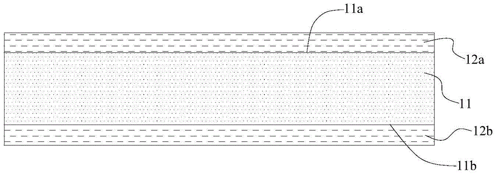
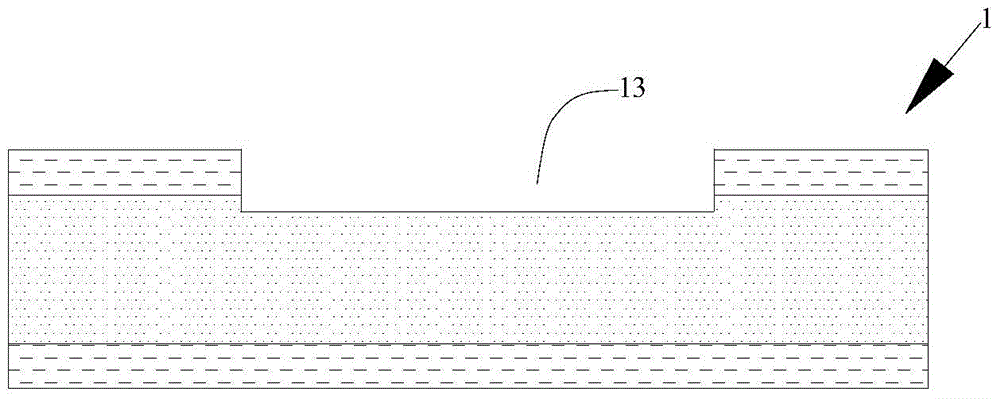
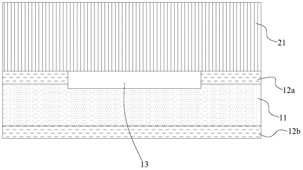
[0046] The MEMS chip 5 of the chip-scale package with multifunctional cover plate of the present embodiment, as Figure 13 As shown, the base substrate 11 comprising a cover plate 30, a MEMS structure layer 22 and at least one lower cavity 13, the area of ​​the cover plate 30 is smaller than the area of ​​the base substrate 11, and the material of the base substrate 11 is crystal oriented heavily doped single crystal silicon, the depth of the lower concave cavity 13 is 5-30 μm, the base substrate 11 has an upper base insulating layer 12a, the material of the upper base insulating layer 12a is silicon dioxide, and the thickness is 0.5-3 μm, The upper base insulating layer 12a is used for bonding the MEMS structure layer 22, providing mechanical support and electrical isolation; the material of the MEMS structure layer 22 is heavily doped single crystal silicon with a crystal orientation, and the MEMS structure layer 22 includes the MEMS structure 22a, The gap 22b and the MEMS...

Embodiment 2

[0069] The cover plate 30 of the chip-scale packaged MEMS chip 5 with the multifunctional cover plate of the present embodiment is used as a constant temperature heater to heat the MEMS chip at a constant temperature: the first metal layer pattern 33 is used as a constant temperature heating resistor 33a, and the constant temperature heating resistor 33a is evenly distributed On the cover plate 30, during subsequent packaging, one end of the constant temperature heating resistor 33a is connected to the seventh ASIC pad 607, and the other end is connected to the fourth ASIC pad 604, as Figure 17 As shown, the power flowing through the constant temperature heating resistor 33a is controlled by the ASIC chip 6. In order to achieve the purpose of constant temperature heating, a thermistor must be provided to feed back the temperature signal. The thermistor is also made of the first metal layer pattern 33. The electrical signal of the resistor is connected to the first ASIC pressur...

Embodiment 3

[0071] For making the thermal convection accelerometer that leak detection is used on cover plate 30, in Figure 12On the cover wafer 3 of the chip-scale packaged MEMS wafer 4 with a multifunctional cover plate shown, an accelerometer pattern is formed by photolithography, an anisotropic etching of the intermetallic insulating layer 34 and an upper cover insulating layer 32a, each Isotropic deep Si etching cover plate substrate 31, deglue, dig out leak detection cavity 82 on the heat convection accelerometer area 81 of cover plate wafer 3, make it into the MEMS wafer for leak detection; In the case of meter area 81, the MEMS wafer for leak detection is cut into a plurality of MEMS chips 8 for leak detection by a method similar to embodiment 1, see Figure 18 .

[0072] Figure 19 The middle heat convection accelerometer area 81 is located at the central position of the cover plate 30. The purpose is to facilitate the protection of the heat convection accelerometer when the M...


PUM

PropertyMeasurementUnit
thicknessaaaaaaaaaa
thicknessaaaaaaaaaa
thicknessaaaaaaaaaa

Abstract

The invention discloses a chip scale packaged MEMS chip with a multifunctional cover board. The MEMS chip comprises the cover board, an MEMS structure layer and a base board underlayer; the cover board comprises a cover board underlayer, an upper cover board insulation layer, a first metal layer pattern, an intermetallic insulation layer and a second metal layer pattern; through holes are arranged in the intermetallic insulation layer; the second metal layer is filled in the through holes; the cover board are bonded with the MEMS structure layer and the upper cover board insulation layer through a sealing ring; and a first bonding block is located on the upper surface of an MEMS signal export part. According to the MEMS chip, the electric signals on the MEMS structure is leaded to the cover board through a metal wire bonded between the first bonding bloc and a second bonding block; then crossover wiring is finished on the cover board; moreover, a constant temperature heater and a thermal convection accelerometer for leakage detection can be manufactured by utilizing the first metal layer pattern and the second metal layer pattern on the cover board; according to the manufacturing method provided by the invention, electric connection between the MEMS structure layer and a base board is unnecessary; it is unnecessary to electrically connect the MEMS structure and the cover board through a TSV (Through Silicon Via); it is unnecessary to carry out crossover wiring in the MEMS structure layer or on the base boar; the process is short; the cost is low; and the yield is high.

Description

technical field [0001] The invention relates to the manufacturing field of MEMS chips, in particular to a chip-level packaged MEMS chip with a multifunctional cover plate, and also relates to the chip-level packaged MEMS chip with a multifunctional cover plate and a manufacturing method thereof. Background technique [0002] MEMS (Micro-Electro-MechanicalSystems) is the abbreviation of Micro-Electro-Mechanical Systems. MEMS chip manufacturing technology uses micro-fabrication technology, especially semiconductor wafer manufacturing technology, to manufacture various micro-mechanical structures, combined with application-specific control integrated circuits (ASICs), composed of Intelligent micro sensors, micro actuators, micro optical devices and other MEMS components. MEMS components have the advantages of small size, low cost, high reliability, strong resistance to harsh environments, low power consumption, high intelligence, easy calibration, and easy integration, and are ...

Claims


Application Information

Patent Timeline
Patent Type & Authority Applications(China)
IPC IPC(8): B81B7/00B81B7/02B81C1/00B81C3/00B81C99/00
CPCB81B7/0009B81B7/007B81B7/0096B81B7/02B81C1/00301B81C1/0069B81C3/001B81C99/0035
Inventor 华亚平
Owner ANHUI BEIFANG XINDONG LIANKE MICROSYST TECH
Why Eureka
Try Eureka