

Method for etching micron silicon through hole
A technology of through-silicon vias and silicon wafers, applied in microstructure technology, microstructure devices, manufacturing microstructure devices, etc., can solve problems such as unfavorable expansion of production, inconvenient operation, etc., and achieve good microscopic appearance and fast etching speed. Effect
- Summary
- Abstract
- Description
- Claims
- Application Information
AI Technical Summary
Problems solved by technology
Method used
Image

Examples
Embodiment 1
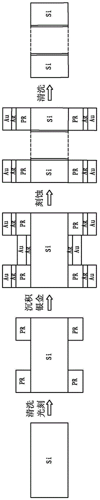
[0033] (1) A silicon wafer with a resistivity of 0.1-1 Ω·cmp and a thickness of 300 μm was ultrasonically cleaned in acetone and ethanol for 5 minutes each, and washed twice. Then wash with hot deionized water and cold deionized water for 2 to 3 times respectively, and blow dry with nitrogen gas for later use.
[0034] (2) Apply photoresist on both sides of the cleaned and dried silicon wafer, bake at 105° C. for 1 minute, expose to photolithography on both sides for 1.4 seconds, and then develop for 45 seconds.
[0035] (3) Using electron beam evaporation equipment, deposit silver with a thickness of 5nm and gold with a thickness of 10nm on the front and back sides of the silicon wafer after photolithography.
[0036] (4) Prepare a 5.74mol / L hydrofluoric acid solution and a 0.46mol / L hydrogen peroxide solution, and mix the two with a volume ratio of 10:1 to prepare a corrosion solution.
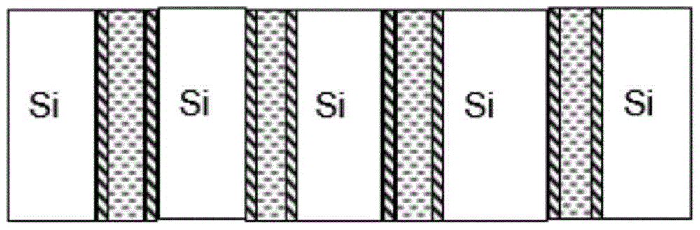
[0037] (5) Put the silicon chip in the step (3) into the prepared etching solution for ...
Embodiment 2
[0040] (1) A silicon wafer with a resistivity of 0.1-1 Ω·cmp and a thickness of 300 μm was ultrasonically cleaned in acetone and ethanol for 5 minutes each, and washed twice. Then wash with hot deionized water and cold deionized water for 2 to 3 times respectively, and blow dry with nitrogen gas for later use.
[0041] (2) Apply photoresist on both sides of the cleaned and dried silicon wafer, bake at 105° C. for 1 minute, expose to photolithography on both sides for 1.4 seconds, and then develop for 45 seconds.
[0042] (3) Using electron beam evaporation equipment, deposit silver with a thickness of 5nm and gold with a thickness of 10nm on the front and back sides of the silicon wafer after photolithography.
[0043] (4) Prepare a 5.74mol / L hydrofluoric acid solution and a 0.46mol / L hydrogen peroxide solution, and mix the two with a volume ratio of 10:1 to prepare a corrosion solution.
[0044] (5) Put the silicon chip in the step (3) into the prepared etching solution for ...
Embodiment 3
[0047] (1) A silicon wafer with a resistivity of 0.01-0.09 Ω·cmp and a thickness of 300 μm was ultrasonically cleaned in acetone and ethanol for 5 minutes each, and cleaned twice. Then wash with hot deionized water and cold deionized water for 2 to 3 times respectively, and blow dry with nitrogen gas for later use.
[0048] (2) Apply photoresist on both sides of the cleaned and dried silicon wafer, bake at 105° C. for 1 minute, expose to photolithography on both sides for 1.4 seconds, and then develop for 45 seconds.
[0049] (3) Using electron beam evaporation equipment, deposit silver with a thickness of 5nm and gold with a thickness of 10nm on the front and back sides of the silicon wafer after photolithography.
[0050] (4) Prepare a 5.74mol / L hydrofluoric acid solution and a 0.46mol / L hydrogen peroxide solution, and mix the two with a volume ratio of 10:1 to prepare a corrosion solution.
[0051] (5) Put the silicon chip in the step (3) into the prepared etching solution...
PUM
| Property | Measurement | Unit |
|---|---|---|
| Thickness | aaaaa | aaaaa |
| Thickness | aaaaa | aaaaa |
| Thickness | aaaaa | aaaaa |
Abstract
Description
Claims
Application Information