Light emitting diode epitaxy structure provided with P-type ohmic contact layer

A technology of ohmic contact layer and light-emitting diode, which is applied in the direction of electrical components, circuits, semiconductor devices, etc., to improve the characteristics of P-type ohmic contact, save production costs, and overcome the difficulty of forming P-type ohmic contact and hole supply.

Active Publication Date: 2016-06-22
ZHIXIN SEMICON (HANGZHOU) CO LTD
View PDF6 Cites 8 Cited by
  • Summary
  • Abstract
  • Description
  • Claims
  • Application Information

AI Technical Summary

Problems solved by technology

[0003] The technical problem to be solved by the present invention is to provide a light-emitting diode epitaxial structure with a P-type ohmic contact layer, which is to grow a layer of semiconductor material with a gradual composition change on the surface of the P-type transmission layer of the LED epitaxial structure, that is, a P-type ohmic contact Layer, its lattice constant increases gradually along the growth direction, and the forbidden band width gradually decreases, thereby generating compressive stress in the entire composition graded layer, and using the polarization effect to generate polarized negative charges through the piezoelectric polarization effect, thereby Attract holes, generate three-dimensional hole gas, increase the hole concentration, reduce the width of the surface depletion region, form a good ohmic contact, improve the P-type ohmic contact characteristics of the LED epitaxial structure, and overcome the existing technology. The wide-forbidden nitride semiconductor is difficult to form P-type ohmic contacts and hole supply defects, which improves the luminous efficiency of LEDs

Method used


Image

  • Light emitting diode epitaxy structure provided with P-type ohmic contact layer
  • Light emitting diode epitaxy structure provided with P-type ohmic contact layer
  • Light emitting diode epitaxy structure provided with P-type ohmic contact layer

Examples


Embodiment 1

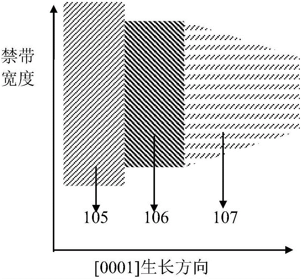
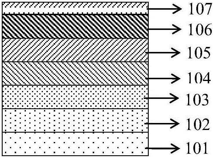
[0033] The light-emitting diode epitaxial structure with a P-type ohmic contact layer in this embodiment includes a sapphire substrate 101, a buffer layer 102 made of AlN material with a thickness of 25 nm, and an N-type AlN material with a thickness of 4 μm from bottom to top. Semiconductor material layer 103, quantum well Al with a quantum barrier AlN thickness of 10 nm 0.8 Ga 0.2 Al with N thickness of 5 nm 0.8 Ga 0.2 Multiple quantum well layer 104 made of N / AlN material, P-type electron blocking layer 105 made of AlN material with a thickness of 50 nm, and Al with a thickness of 150 nm 0.9 Ga 0.1 P-type semiconductor material transport layer 106 of N material and Al with a thickness of 10 nm x Ga 1-x For the P-type ohmic contact layer 107 made of N material, where x is linearly graded from 0.9 to 0, its lattice constant gradually increases along the growth direction, and the forbidden band width gradually decreases.

[0034] The light-emitting diode epitaxial struct...

Embodiment 2

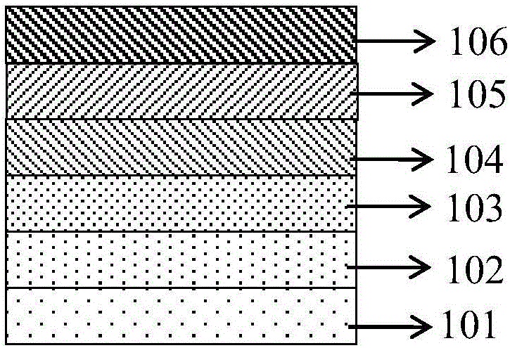
[0042] The light-emitting diode epitaxial structure with a P-type ohmic contact layer of this embodiment includes a Si substrate 101 and Al with a thickness of 10 nm from bottom to top. 0.2 In 0.3 Ga 0.5 Buffer layer 102 of N material, Al with a thickness of 2 μm 0.1 In 0.5 Ga 0.4 N-type semiconductor material layer 103 made of N material, quantum well In with a quantum barrier GaN thickness of 10 nm 0.8 Ga 0.2 In with N thickness of 5 nm 0.8 Ga 0.2 A multiple quantum well layer 104 made of N / GaN material, a P-type electron blocking layer 105 made of AlN material with a thickness of 10 nm, a P-type semiconductor material transport layer 106 made of AlN material with a thickness of 100 nm, and Al with a thickness of 150 nm x In y Ga 1-x-y P-type ohmic contact layer 107 made of N material, in the formula, the first 100nm growth keeps y=0, and x gradually changes from 0.9 to 0; the last 50nm growth keeps x=0, y changes nonlinearly from 0 to 0.1, and the whole P The -typ...

Embodiment 3

[0051] The light-emitting diode epitaxial structure with a P-type ohmic contact layer in this embodiment includes a SiC substrate 101, a GaN buffer layer 102 with a thickness of 50 nm, and an N-type GaN material with a thickness of 8 μm from bottom to top. A semiconductor material layer 103, a quantum well In with a quantum barrier GaN thickness of 10 nm 0.8 Ga 0.2 In with N thickness of 5 nm 0.8 Ga 0.2 Multiple quantum well layer 104 made of N / GaN material, Al with a thickness of 100 nm 0.2 Ga 0.8 P-type electron blocking layer 105 of N material, P-type semiconductor material transport layer 106 of GaN material with a thickness of 500 nm, and In x Ga 1-x P-type ohmic contact layer 107 made of N material, in the formula, the first 100nm growth x linearly changes from 0 to 0.2, and the last 100nm growth x linearly changes from 0.2 to 1, so that its lattice constant gradually increases along the growth direction, and the forbidden The tape width gradually decreases.

[00...


PUM


Abstract

The invention discloses a light emitting diode epitaxy structure provided with a P-type ohmic contact layer and relates to a semiconductor device which is characterized by the electrode, is provided with at least one potential jump barrier or surface barrier and is special for light emission. The structure comprises a substrate, a buffer layer, an N-type semiconductor material layer, a multiple quantum well layer, a P-type electron blocking layer, a P-type semiconductor material transport layer and the P-type ohmic contact layer from top to bottom in sequence, wherein the P-type ohmic contact layer consists of AlxInyGa1-x-yN, wherein x is not less than 0 and is less than 1, y is not less than 0 and is less than 1, 1-x-y is not less than 0, the group component is gradient, the lattice constant is gradually increased along the growth direction and the forbidden bandwidth is gradually reduced. The light emitting diode epitaxy structure overcomes the defects that the wideband gap nitride semiconductor is difficult to form P-type ohmic contact and the hole supply is difficult in the prior art, and the light emitting efficiency of the LED is improved.

Description

technical field [0001] The technical solution of the present invention relates to a semiconductor device with at least one potential jumping barrier or surface potential barrier characterized by an electrode, which is specially suitable for light emission, specifically a light emitting diode epitaxial structure with a P-type ohmic contact layer. Background technique [0002] Because light-emitting diodes have the advantages of energy saving, environmental protection, flexible design, and long life, they have developed rapidly in recent years. In particular, the success of III-V nitride semiconductor LED technology in the field of blue light has directly promoted the entry of LED lighting into thousands of households. Currently, nitride LEDs are moving towards shorter wavelengths (ultraviolet, deep ultraviolet) and longer wavelengths (green, yellow). The ohmic contact characteristics of LEDs directly affect the efficiency and reliability of the entire device. However, the a...

Claims


Application Information

Patent Timeline
Patent Type & Authority Applications(China)
IPC IPC(8): H01L33/40H01L33/36H01L33/02
CPCH01L33/02H01L33/36H01L33/40
Inventor 张紫辉张勇辉毕文刚徐庶耿翀
Owner ZHIXIN SEMICON (HANGZHOU) CO LTD
Why Eureka
Try Eureka