Method for measuring layer number of graphene on silicon carbide substrate

A measurement method, graphene technology, applied in the field of spectral analysis, can solve problems such as the inability to quickly, accurately, and directly measure the number of graphene layers, and the difficulty of accurately measuring the thickness of nanoscale films, so as to facilitate device processing and performance testing Effect

Inactive Publication Date: 2016-06-29
天津恒电空间电源有限公司 +1
View PDF4 Cites 5 Cited by
  • Summary
  • Abstract
  • Description
  • Claims
  • Application Information

AI Technical Summary

Problems solved by technology

However, traditional thin-film detection instruments such as step meters are difficult to accurately measure the thickness of nano-sized films; transmission electron microscopy is a relatively intuitive detection method, but the opacity of the silicon carbide substrate greatly limits the application of this technology; pull Mann spectroscopy and atomic force microscopy are more suitable for graphene obtained by mechanical exfoliation. If they are used

Method used


Image

  • Method for measuring layer number of graphene on silicon carbide substrate
  • Method for measuring layer number of graphene on silicon carbide substrate
  • Method for measuring layer number of graphene on silicon carbide substrate

Examples


Embodiment 1

[0026] A method for measuring the number of layers of graphene on a silicon carbide substrate, comprising the following measurement steps:

[0027] (1) Using 4H-SiC as the substrate, a certain number of layers of graphene was grown on the silicon surface of the substrate by pyrolytic epitaxy.

[0028] (2) Carry out 30s nitrogen purging to the graphene sample surface, to remove attached dust and impurity particles.

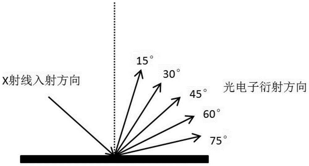
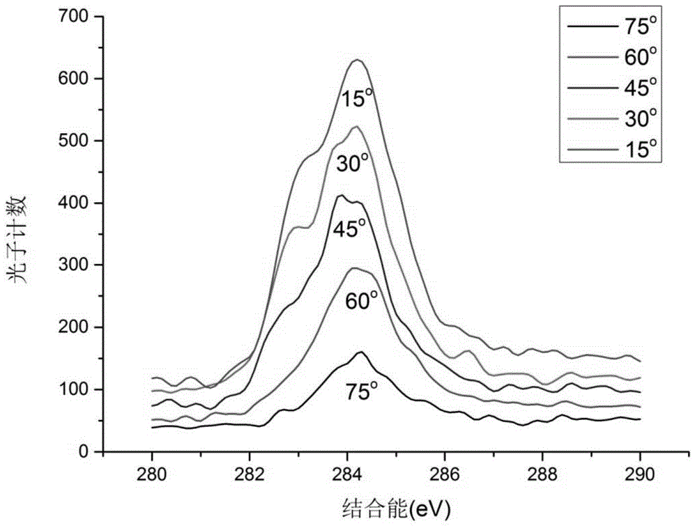
[0029] (3) Measure the XPS energy spectrum of the sample, and scan the energy range from 280eV to 290eV. The incident angle of X-ray is 45°, the diffraction acceptance angle of photoelectron is θ, the values ​​are 15°, 30°, 45°, 60°, 75° respectively, record the XPS energy spectrum of the sample when different θ values ​​are selected, Energy spectrum such as figure 2 shown.

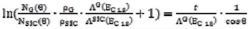
[0030] (4) Calculate the integrated intensity of the peaks at 284.5eV and 282.9eV according to the XPS spectrum obtained from the measurement. Among them, 284.5eV is the binding energy of...


PUM


Abstract

The invention relates to a method for measuring the layer number of graphene on a silicon carbide substrate. The invention belongs to the technical field of spectral analysis. The method comprises 1, forming a graphene sample with a multilayer structure and a certain thickness on a silicon surface of silicon carbide through a thermal decomposition epitaxy method, 2, measuring the sample through an X ray photoelectron spectroscopy, 3, calculating C1s electron diffraction photon integrated intensity in a C-C bond at 284.5eV and C1s electron diffraction photon integrated intensity in a Si-C bond at 282.9eV through a scanned XPS energy spectrum, 4, substituting the diffraction photon integrated intensities into a function equation of the diffraction photon integrated intensity and graphene thickness and calculating sample graphene thickness and 5, comparing the graphene thickness and graphene atom interlayer space to obtain the layer number of the graphene sample. The method is fast, realizes accurate measurement, is free of peeling of graphene from a substrate, realizes lossless measurement and is convenient for device processing and performance test.

Description

technical field [0001] The invention belongs to the technical field of spectral analysis, in particular to a method for measuring the number of layers of graphene on a silicon carbide substrate. Background technique [0002] As a new type of nanomaterial, graphene has extremely superior properties in the fields of light, electricity and magnetism. Graphene and C 60 Like diamond, they are all allotropes of carbon, and carbon atoms are represented by sp 2 The hybridization method forms a bond to form a hexagonal structure similar to a honeycomb, and the hexagonal planes are stacked layer by layer to form a nanomaterial with a special energy band structure - graphene. [0003] At present, growing graphene on the surface of silicon carbide has become a relatively mature means of preparing graphene. Under certain conditions, the silicon atoms on the surface of silicon carbide are removed, and the remaining carbon atoms follow the principle of the lowest energy to self-assemble ...

Claims


Application Information

Patent Timeline
IPC IPC(8): G01N23/20
Inventor 孙希鹏杜永超梁存宝铁剑锐王鑫
Owner 天津恒电空间电源有限公司
Why Eureka
Try Eureka