Composite substrate for fabricating flexible display, fabrication method of composite substrate and fabrication method of active matrix/organic light emitting diode (AMOLED)

A composite substrate, flexible display technology, used in semiconductor/solid-state device manufacturing, electrical components, electric solid-state devices, etc., can solve the problem that flexible substrates and adhesives are not resistant to high temperature, no flexible display substrates, and damage to flexible substrates and carriers. Substrate adhesion and other issues, to achieve the effect of improving convenience, bonding stability, and reducing substrate warpage

Inactive Publication Date: 2016-07-20
SHENZHEN TCL IND RES INST
View PDF6 Cites 17 Cited by
  • Summary
  • Abstract
  • Description
  • Claims
  • Application Information

AI Technical Summary

Problems solved by technology

In the process of preparation, the flexible substrate and adhesive have the disadvantage of not being resistant to high temperature: such as general flexible substrates such as PET (polyethylene terephthalate), PEN (polyethylene naphthalate) and other materials Restricted by the heat treatment temperature, it is only suitable for low-temperature flexible displays; at the same time, high temperature will destroy the adhesion between the flexible substrate and the carrier substrate
Therefore, there is no flexible display substrate that can realize high-temperature TFT process in the existing S2S process

Method used


Image

  • Composite substrate for fabricating flexible display, fabrication method of composite substrate and fabrication method of active matrix/organic light emitting diode (AMOLED)
  • Composite substrate for fabricating flexible display, fabrication method of composite substrate and fabrication method of active matrix/organic light emitting diode (AMOLED)
  • Composite substrate for fabricating flexible display, fabrication method of composite substrate and fabrication method of active matrix/organic light emitting diode (AMOLED)

Examples


preparation example Construction

[0046] Further, the present invention also proposes the above-mentioned preparation method of the composite substrate for flexible display manufacturing, including the following steps:

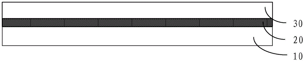
[0047] S10a, obtaining the hard substrate 10, and performing surface activation treatment on the hard substrate 10;

[0048] S20a, coating the resin solution of the high temperature resistant thin film layer 20 on the activated surface of the hard substrate 10 to form the high temperature resistant thin film layer 20;

[0049] S30a, drying the hard substrate 10 coated with the high temperature-resistant thin film layer 20 after standing in a vacuum;

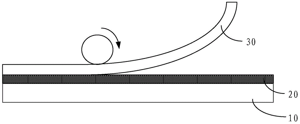
[0050] S40a, attaching the resin casting film of the high temperature resistant flexible substrate layer 30 to the surface of the dried high temperature film layer 20 to form the high temperature resistant flexible substrate layer 30;

[0051] S50a, the hard substrate 10 with the high temperature resistant flexible substrate layer 30 is subjecte...

Embodiment 1

[0084] In this embodiment 1, a phthalic anhydride-type PI resin material is used to realize the preparation of the composite layer, and a high-brightness glass plate is selected as the hard substrate.

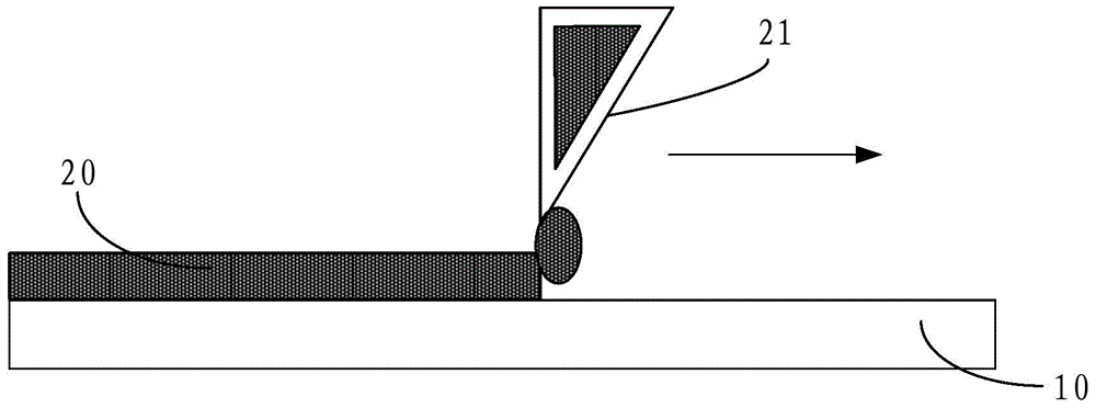
[0085] S10, ultrasonically cleaning the glass plate, and then performing plasma treatment on the surface of the glass plate with nitrogen after cleaning;

[0086] S20, use NMP (N-methylpyrrolidone) as a solvent to form a viscous solution with PI resin, and pour the solution into the inner cavity of the squeegee; fix the glass plate in a class 100 clean room, and keep the squeegee with the squeegee With a distance of 0mm-2mm on the surface of the glass plate, scrape slowly and uniformly to form a high-temperature resistant film layer; after the scrape coating is completed, use a rotary machine to rotate the glass plate to the high-temperature resistant film layer to form a flat and uniform film with a thickness of 2μm-5μm;

[0087] S30, after the coating is completed, quickly tr...

Embodiment 2

[0095] In this embodiment 2, a biphenyl type PI resin material is used to realize the preparation of the composite layer, and a silicon wafer is selected as the hard substrate.

[0096] S10, after ultrasonically cleaning the silicon wafer, performing argon plasma treatment on the surface of the silicon wafer with a plasma surface treatment machine;

[0097] S20, use DMAc (dimethylacetamide) as a solvent to form a viscous solution with PI resin, and pour the solution into the inner cavity of the scraping knife; fix the silicon wafer in a class 100 clean room, keep the scraping knife and With a distance of 0mm-2mm on the surface of the silicon wafer, scrape slowly and uniformly to form a high-temperature resistant film layer; after the scrape coating is completed, use a rotary machine to rotate the silicon wafer to the high-temperature resistant film layer to form a flat and uniform film with a thickness of 2μm-5μm;

[0098] S30, after the coating is completed, quickly transfer ...


PUM

PropertyMeasurementUnit
thicknessaaaaaaaaaa
thicknessaaaaaaaaaa

Abstract

The invention provides a composite substrate for fabrication of flexible display. The composite substrate comprises a hard substrate, wherein a high-temperature resistant flexible substrate layer is arranged on the surface of the hard substrate, a high-temperature resistant thin film layer is arranged between the high-temperature resistant flexible substrate layer and the hard substrate, and the bonding force between the high-temperature resistant thin film layer and the hard substrate is larger than that between the high-temperature resistant thin film layer and the high-temperature resistant flexible substrate layer. In a flexible display thin film transistor (TFT) process of the composite substrate, a flexible substrate and the hard substrate are connected by the high-temperature resistant thin film layer on the hard substrate and a composite layer structure of the high-temperature resistant flexible substrate layer without the adoption of a binding agent, and the bonding force between layers is moderate; the material selects a high-temperature resistant material, so that the mass production of a flexible active matrix/organic light emitting diode (AMOLED) display device by a high-temperature FTF process is achieved; and moreover, the difference of the binding force between layers can be used for facilitating the striping of the flexible substrate after a high temperature.

Description

technical field [0001] The invention belongs to the technical field of flexible displays, and in particular relates to a composite substrate used for flexible display manufacturing, a preparation method thereof, and an AMOLED manufacturing method. Background technique [0002] Currently, there are two main types of manufacturing display devices on flexible substrates: R2R (roll to roll, roll-to-roll) production process and S2S (sheet to sheet, sheet-to-sheet) production process; among them, in the R2R process, the soft board is first rolled from a cylindrical After the material roll is rolled out, add special-purpose functions on the soft board or process on the surface of the soft board, and finally roll the soft board into a cylindrical shape or directly cut the finished product; this method mainly adopts the method of printing on the soft board Display devices are prepared on flexible substrates, but due to the limitations of printing technology and display ink materials,...

Claims


Application Information

Patent Timeline
Patent Type & Authority Applications(China)
IPC IPC(8): H01L51/00H01L51/52H01L51/56
Inventor 高卓付东
Owner SHENZHEN TCL IND RES INST
Why Eureka
Try Eureka