

Enhanced fin-type insulated gate high-electronic mobility transistor
A technology with high electron mobility and insulated gates, applied in circuits, electrical components, semiconductor devices, etc., can solve problems such as large sub-threshold swings, unfavorable nanoscale digital integrated circuits, and severe short channel effects, and achieve enhanced gate controllability, low gate leakage current, and the effect of suppressing short channel effects
- Summary
- Abstract
- Description
- Claims
- Application Information
AI Technical Summary
Problems solved by technology
Method used
Image

Examples
Embodiment 1
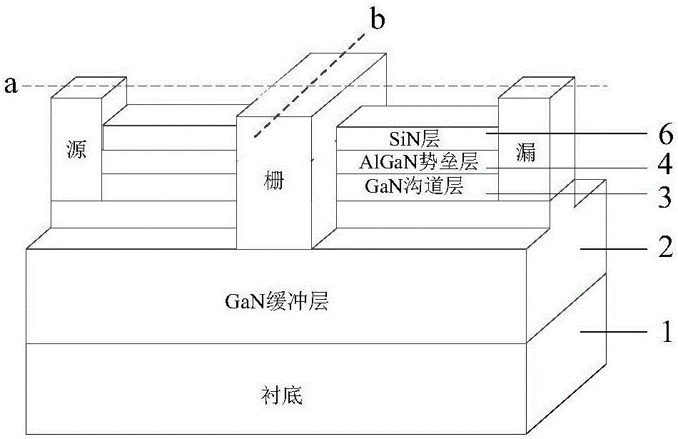
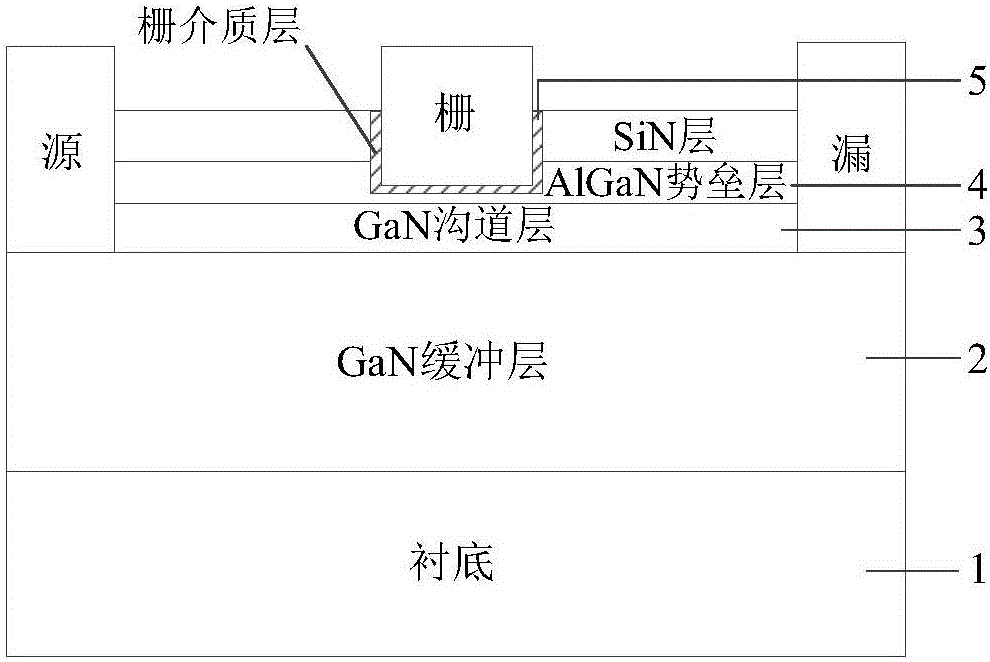
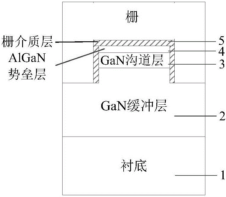
[0041] Example 1: Fabrication of a fin-type AlGaN / GaN heterojunction with a width of 200nm and a groove gate depth of 8nm enhanced fin-type insulated gate high electron mobility crystal.
[0042] Step 1: growing a buffer layer.
[0043] At a temperature of 700°C and a pressure of 1.5×10 4 Under the process conditions of Pa, the use of metal organic compound chemical vapor deposition MOCVD equipment in Figure 4 A GaN buffer layer with a thickness of 1 μm is grown on the SiC substrate shown in (a), and the reaction gases are trimethylgallium and ammonia.
[0044] Step 2: growing a channel layer.
[0045] At a temperature of 850°C and a pressure of 1.5×10 4 Under the process conditions of Pa, a 5nm-thick GaN channel layer is grown on the GaN buffer layer by using metal organic compound chemical vapor deposition MOCVD equipment, and the reaction gases are trimethylgallium and ammonia.
[0046] Step 3: growing a barrier layer.
[0047] At a temperature of 950°C and a pressure...
Embodiment 2
[0065] Example 2: Fabrication of a fin-type AlGaN / GaN heterojunction with a width of 300nm and a groove gate depth of 5nm enhanced fin-type insulated gate high electron mobility crystal.
[0066] Step A: growing a buffer layer on the substrate.
[0067] A layer of GaN buffer layer with a thickness of 1.5 μm was grown on the SiC substrate by metal organic compound chemical vapor deposition MOCVD equipment. The growth process conditions were: temperature 700 ° C, pressure 1.5 × 10 4 Pa, the reaction gas is trimethylgallium and ammonia.
[0068] Step B: growing a channel layer on the buffer layer.
[0069] The implementation of this step is the same as step 2 of Embodiment 1.
[0070] Step C: growing a barrier layer on the channel layer.
[0071] Using metal organic compound chemical vapor deposition MOCVD equipment to grow an AlGaN barrier layer with a thickness of 15nm and an Al composition of 30% on the GaN channel layer, the GaN channel layer and the AlGaN barrier layer fo...
Embodiment 3
[0086] Example 3: Fabrication of a fin-type AlGaN / GaN heterojunction with a width of 250nm and a groove gate depth of 7nm enhanced fin-type insulated gate high electron mobility crystal.
[0087] Step 1: Growth buffer layer.
[0088] A layer of GaN buffer layer with a thickness of 1.5 μm was grown on the SiC substrate using metal organic compound chemical vapor deposition MOCVD equipment. The growth process conditions were: temperature 700 ° C, pressure 1.5 × 10 4 Pa, the reaction gas is trimethylgallium and ammonia.
[0089] Step 2: growing a channel layer.
[0090] The implementation of this step is the same as step 2 of Embodiment 1.
[0091] Step 3: Growing a barrier layer.
[0092] On the GaN channel layer, use metal organic compound chemical vapor deposition MOCVD equipment to grow an AlGaN barrier layer with a thickness of 17nm and an Al composition of 27%. The GaN channel layer and the AlGaN barrier layer form an AlGaN / GaN heterojunction , A two-dimensional electro...
PUM
| Property | Measurement | Unit |
|---|---|---|
| Thickness | aaaaa | aaaaa |
| Thickness | aaaaa | aaaaa |
| Thickness | aaaaa | aaaaa |
Abstract
Description
Claims
Application Information