Gallium nitride-based light emitting diode and preparation method thereof

A light-emitting diode, gallium nitride-based technology, applied in electrical components, circuits, semiconductor devices, etc., can solve the problems of reducing the effective barrier height of the electron blocking layer, reducing the blocking ability of the electron blocking layer, and increasing the effective barrier of the valence band, etc. , to improve the electron blocking ability, weaken the energy band bending effect, and improve the droop effect.

Active Publication Date: 2016-08-03
TIANJIN SANAN OPTOELECTRONICS
View PDF3 Cites 16 Cited by
  • Summary
  • Abstract
  • Description
  • Claims
  • Application Information

AI Technical Summary

Problems solved by technology

figure 2 It shows the energy band structure diagram of conventional commercial gallium polar gallium nitride-based LEDs. The electron blocking layer 104 generates positive charges at the interface due to tensile strain, causing the energy band to bend downward, so that the effective potential of the electron blocking layer in the conduction band is The barrier height is reduced, and the effective potential barrier in the valence band is increased, which not only reduces the electron blocking ability of the electron blocking layer, but also increases the potential barrier for holes injected into the multi-quantum well light-emitting layer on the p-type side.

Method used


Image

  • Gallium nitride-based light emitting diode and preparation method thereof
  • Gallium nitride-based light emitting diode and preparation method thereof
  • Gallium nitride-based light emitting diode and preparation method thereof

Examples


Embodiment 1

[0036] The invention provides a gallium nitride-based LED with high light efficiency and a preparation method thereof. The preparation process mainly includes the following steps:

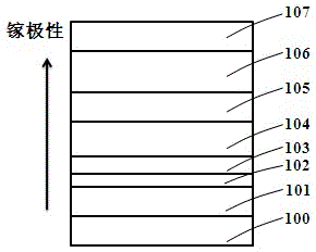
[0037] attached image 3 A high-efficiency gallium nitride-based LED prepared by the present invention is illustrated, which are as follows from bottom to top: substrate 100, gallium polar low-temperature buffer layer 101, gallium polar non-doped nitride layer 102, gallium polar N-type Nitride layer 103 , gallium polar multiple quantum well light emitting layer 104 , nitrogen polar electron blocking layer 205 , nitrogen polar P-type nitride layer 206 , nitrogen polar P-type nitride contact layer 207 .

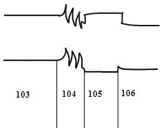
[0038] Figure 4 The energy band structure diagram of the above-mentioned high-efficiency GaN-based LED is shown. and figure 2 Compared with the energy band structure diagram of the conventional commercial gallium polar gallium nitride-based LED shown, in the above structure, the polarized charg...

Embodiment 2

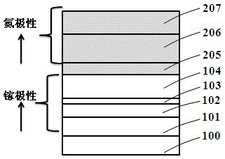
[0050] This embodiment is different from Embodiment 1 in that: the P-type nitride layer and the P-type nitride contact layer are Ga polar. Using gallium-polarity P-type nitride layer and P-type nitride contact layer behind the nitrogen-polarity electron blocking layer can make the surface of the device smoother, which is beneficial to the electrode preparation of the subsequent chip process, such as Figure 5 .

[0051] In this embodiment, the gallium polar low temperature buffer layer 101, the gallium polar non-doped nitride layer 102, the gallium polar N-type nitride layer 103, the gallium polar multilayer After the quantum well light-emitting layer 104, the substrate is transferred to a molecular beam epitaxy reaction chamber to grow a nitrogen polar electron blocking layer 205, a gallium polar P-type nitride layer 306 and a gallium polar P-type nitride contact layer 307. Wherein the nitrogen-polar electron blocking layer 205 is grown under nitrogen-rich conditions, and it...


PUM


Abstract

The invention provides a gallium nitride-based light emitting diode with high luminous efficiency and a preparation method thereof, and belongs to the field of photoelectric device preparation. The LED can maintain higher photoelectric conversion efficiency and a lower Droop effect under bulk current injection. The LED comprises a bottom layer and a light emitting layer which are grown through an MOCVD technology and a P-type layer which is grown through a molecular beam epitaxy technology, namely, a gallium polar buffer layer, a non-doped nitride layer, an N-type nitride layer and a multiple-quantum-well light emitting layer are grown through the MOCVD technology, and then, a sample is transferred to the reaction chamber of molecular beam epitaxy equipment, and a nitrogen polar electron blocking layer, a P-type nitride layer and a P-type nitride contact layer are grown. Through the method, band bending caused by polarization between the electron blocking layer and the multiple-quantum-well light emitting layer is reduced, the barrier height of electron overshoot to the P-type layer is increased, and the barrier height of hole injection to the multiple-quantum-well region is reduced.

Description

technical field [0001] The invention relates to the field of semiconductor optoelectronic device preparation, in particular to a preparation technology of gallium nitride-based LED with high light efficiency. Background technique [0002] The rapid development of wide bandgap III-V semiconductor materials has enabled the commercialization of high-brightness light-emitting diodes from green to near-ultraviolet. However, most of the current commercial LEDs are prepared by growing 001-plane nitrides on sapphire, silicon carbide or silicon substrates by MOCVD technology, and the surfaces are gallium polar planes. [0003] figure 1 A structure diagram of a conventional commercial gallium polar gallium nitride-based LED is shown, in which there is a strong polarization field between the multi-quantum well light-emitting layer 104 and the electron blocking layer 105 due to the difference in lattice constant. figure 2 It shows the energy band structure diagram of conventional com...

Claims


Application Information

Patent Timeline
Patent Type & Authority Applications(China)
IPC IPC(8): H01L33/14H01L33/06H01L33/32H01L33/00
CPCH01L33/06H01L33/00H01L33/14H01L33/32H01L33/145H01L33/007
Inventor 张东炎刘文叶大千刘晓峰高文浩王笃祥
Owner TIANJIN SANAN OPTOELECTRONICS
Why Eureka
Try Eureka