Method for preparing porous organic semiconductor film by using solution method and application thereof

A technology of organic semiconductors and semiconductors, applied in measuring devices, instruments, and material analysis through electromagnetic means, to achieve the effects of easy operation, simple methods, and low cost

Active Publication Date: 2016-08-10
黄山市开发投资集团有限公司
View PDF3 Cites 11 Cited by
  • Summary
  • Abstract
  • Description
  • Claims
  • Application Information

AI Technical Summary

Problems solved by technology

Among them, the preparation of porous organic semiconductor thin films can only be realized by evaporation and a series of complicated process design.

Method used


Image

  • Method for preparing porous organic semiconductor film by using solution method and application thereof
  • Method for preparing porous organic semiconductor film by using solution method and application thereof
  • Method for preparing porous organic semiconductor film by using solution method and application thereof

Examples


Embodiment 1

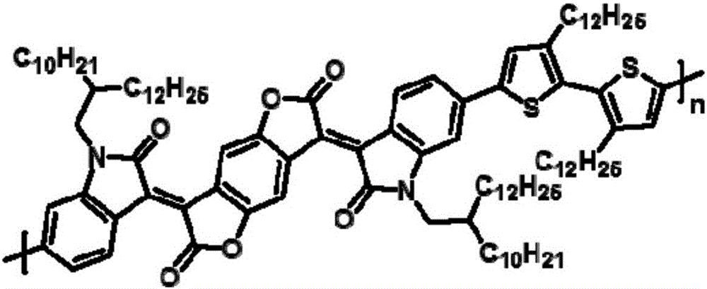
[0048] The present embodiment is based on isoindigo polymer isomer derivative PBIBDF-BT (structural formula such as figure 1) is a high-molecular-weight organic semiconductor (its weight-average molecular weight is 58852), with poly(1,4) butanediol adipate (PBA) (structural formula as shown in formula (16)) as a blended low-molecular-weight Oligomers (with a weight-average molecular weight of 2000), on Cytop-modified SiO 2 Porous PBIBDF-BT films were prepared on the substrate.

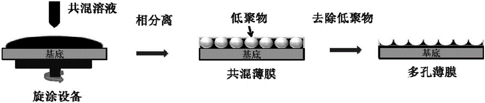
[0049] Such as figure 2 As shown, the preparation steps of the porous PBIBDF-BT film of the present embodiment are as follows:

[0050] with 300nm SiO 2 The heavily doped silicon wafer of the first layer is used as the substrate, which is washed with acetone, ethanol, and deionized water for 15 minutes in sequence, and then treated with ozone for 15 minutes. Subsequently, the Cytop solution was spin-coated on the substrate at a speed of 3000r / min for about 1min, and then placed on a hot stage at 1...

Embodiment 2

[0054] In this embodiment, the isoindigo polymer isomer derivative PBIBDF-BT (its weight average molecular weight is 55200) is a high molecular weight organic semiconductor, and polydimethylsiloxane (silicon oil for short, its structural formula is as formula (18) ) shown) as a blended low molecular weight oligomer (its weight-average molecular weight is 3000), a porous PBIBDF-BT film is prepared on a silicon substrate modified by octadecyltrichlorosilane (OTS), and by adjusting The content of oligomers is used to control the pore size in porous membranes. Specific steps are as follows:

[0055] Place the silicon substrate in H 2 SO 4 / H 2 o 2 (Volume ratio 7:3) was washed in the mixed solution at 150°C, and then the substrate was soaked in 20mL dry toluene dripped with 0.05mL OTS for 20min, so that the surface self-assembled a layer of hydrophobic OTS modified layer to obtain OTS-modified Silicon substrate.

[0056] PBIBDF-BT and silicone oil were weighed according to 1...

Embodiment 3

[0059] This embodiment prepares the porous organic semiconductor film in the same manner as in Example 1, the only difference is that PBIBDF-BT is replaced by PIID-BT polymer (its molecular formula is as follows: Figure 5 , its weight-average molecular weight is 65560), obtains the porous PIID-BT thin film.

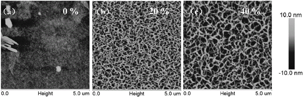
[0060] The AFM figure of the porous PIID-BT film obtained in this embodiment is as follows Figure 6 As shown, it can be seen from the figure that a porous membrane is formed.


PUM


Abstract

The invention discloses a method for preparing porous organic semiconductor film by using a solution method and application thereof. The method is characterized by including: dissolving organic semiconductor with high molecular weight and oligomer with low molecular weight in an organic solvent to obtain a blending solution; spin-coating the blending solution on the substrate to form a blending film by a solution spin-coating method, and using an appropriate solvent to dissolve and remove the oligomer with low molecular weight in the blending film to obtain the porous organic semiconductor film. The porous film is prepared by the solution method, and the method is simple, has good repeatability, has low requirements of the device and technology condition, and is suitable for preparing most of the high-molecular semiconductor porous films. The porous organic semiconductor film prepared by the invention can be used for the gas phase sensor, and can significantly improve the detection effect of the organic semiconductor material on the corresponding gas analyte by means of providing an effective gas dispersion channel.

Description

technical field [0001] The invention belongs to the field of organic semiconductor thin films and devices, in particular to a new method for preparing porous organic semiconductor thin films and its application in chemical gas phase sensors. Background technique [0002] A class of organic compound film materials with conductivity between organic insulators and organic conductors is called organic semiconductor films, which are mainly used in organic field effect transistors (OFETs), organic solar cells (OSCs), organic light-emitting diodes (OLEDs) and organic semiconductors. The active layer of devices such as sensors (Organic Sensor). Among them, the porous organic semiconductor thin film with porous structure is applied to the chemical gas phase sensor because it can significantly enhance the gas phase detection capability. [0003] The morphology and microstructure of organic semiconductor thin films largely determine the performance of devices. Traditional methods for ...

Claims


Application Information

Patent Timeline
Patent Type & Authority Applications(China)
IPC IPC(8): G01N27/12
CPCG01N27/126
Inventor 邱龙臻吴少华王庆贺葛丰薛战
Owner 黄山市开发投资集团有限公司
Why Eureka
Try Eureka