Contacting passivation crystalline silicon solar cell structure and preparation method

A technology of solar cells and crystalline silicon, applied in the field of solar cells, can solve the problems of high recombination at the opening and only battery efficiency.

Inactive Publication Date: 2016-08-10
CHANGZHOU UNIV +1
View PDF3 Cites 8 Cited by
  • Summary
  • Abstract
  • Description
  • Claims
  • Application Information

AI Technical Summary

Problems solved by technology

[0002] Surface passivation of crystalline silicon solar cells is an important method to improve crystalline silicon solar cells. PERC and PERL cells based on silicon oxide, aluminum oxide, and dielectric films have been commercialized. However, these cells require local openings and openings. In 2013, Fraunhofer ISE developed

Method used


Image

  • Contacting passivation crystalline silicon solar cell structure and preparation method
  • Contacting passivation crystalline silicon solar cell structure and preparation method

Examples


Embodiment 1

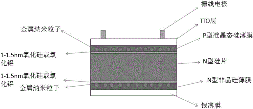
[0036] 1. Polish the 180um P-type silicon wafer on both sides, and then perform RCA cleaning

[0037] 2. Double-sided aluminum oxide film is prepared by ALD with a thickness of 1-1.5nm; hot nitric acid oxidation or ultraviolet ozone treatment can also be used to form a silicon oxide film of 1-1.5nm.

[0038] 3. A 50nm gold thin film is prepared by thermal evaporation on both sides of the silicon wafer, and then annealed at 400 degrees to form metal nanoparticles. The annealing process can also enhance the passivation effect of the passivation film.

[0039] 4. Prepare an N-type quasi-crystalline silicon film on the light-receiving surface with a thickness of 10nm; the method used is PECVD. The quasi-crystalline silicon film is a film between amorphous and microcrystalline close to the microcrystalline silicon phase, which can be adjusted by adjusting The preparation process is obtained, and then the 70nm ITO film is prepared by electron beam evaporation or sputtering, and fina...

Embodiment 2

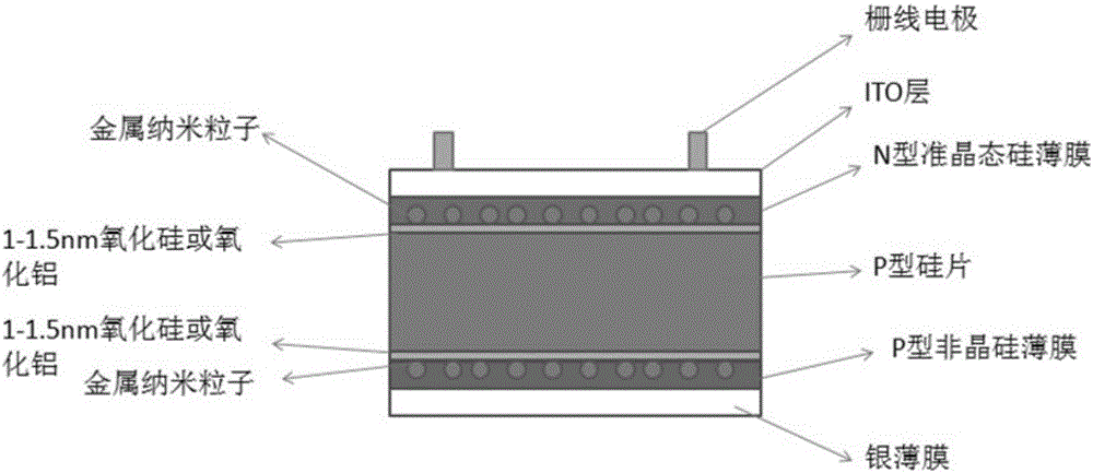
[0042] 1. Polish the 180um N-type silicon wafer on both sides, and then perform RCA cleaning.

[0043] 2. Double-sided aluminum oxide film is prepared by ALD, with a thickness of 1-1.5nm. It can also be oxidized with hot nitric acid, or treated with ultraviolet and ozone to form a silicon oxide film of 1-1.5nm.

[0044] 3. A 100nm gold film is prepared by thermal evaporation on both sides of the silicon wafer, and then annealed at 400 degrees to form metal nanoparticles. The annealing process can also enhance the passivation effect of the passivation film.

[0045] 4. Prepare a P-type quasi-crystalline silicon film on the light-receiving surface with a thickness of 15nm. The method used is PECVD. The quasi-crystalline silicon film is a film between amorphous and microcrystalline close to the microcrystalline silicon phase. It can be obtained by adjusting the preparation process, and then the 80nm ITO film is prepared. The method used is electron beam evaporation. Or sputterin...


PUM

PropertyMeasurementUnit
Thicknessaaaaaaaaaa
Diameteraaaaaaaaaa
Thicknessaaaaaaaaaa

Abstract

The invention belongs to the technical field of solar cells and relates to a contacting passivation crystalline silicon solar cell structure and preparation method. Double face polishing of an N or P type crystal silicon wafer is performed and then double face silicon oxide layer or aluminum oxide preparation is performed; than double face golden or silver nano particle preparation is performed; back face non-crystalline silicon N (P) type layer preparation is performed; light receiving face quasi crystalline state P (N) type silicon film preparation is performed; 70 nm thick ITO film and grid electrode is prepared on the P (N) type silicon film; and back face silver film preparation is performed. The invention has beneficial effects that metal nano particles wrapped by a passivation coating realizes an effect of a carrier tunneling channel, so that the carrier tunneling channel effect is improved, the fill factors of a crystalline silicon solar cell can be increased integrally and the surface plasma effect of the metal nano particles realizes an antireflection effect.

Description

technical field [0001] The patent of the invention belongs to the technical field of solar cells, and relates to a structure and a preparation method of a contact passivation crystalline silicon solar cell. Background technique [0002] Surface passivation of crystalline silicon solar cells is an important method to improve crystalline silicon solar cells. PERC and PERL cells based on silicon oxide, aluminum oxide, and dielectric films have been commercialized. However, these cells require local openings and openings. In 2013, Fraunhofer ISE developed a tunnel oxide passivation contact (TOPCon) technology. This technology uses an ultra-thin oxide layer and silicon film to passivate the back of the battery. The oxide layer is grown by wet chemical method with a thickness of 1.4nm. Then, 20nm phosphorus-doped amorphous silicon is deposited on the oxide layer, followed by annealing. Enhance passivation effect. However, this method only passivates the back of the battery, and ...

Claims


Application Information

Patent Timeline
IPC IPC(8): H01L31/042H01L31/18H01L31/0216
CPCH01L31/0216H01L31/042Y02E10/50Y02P70/50
Inventor 丁建宁袁宁一王书博程广贵
Owner CHANGZHOU UNIV
Why Eureka
Try Eureka