Graphene electro-optical modulator and preparation method thereof
An electro-optical modulator and graphene technology, applied in the field of optical modulation, can solve the problems of limiting the application of graphene electro-optical modulators, large insertion loss of waveguides, etc., achieving controllable pulse repetition frequency, tunable pulse width, and avoiding insertion loss. Effect
- Summary
- Abstract
- Description
- Claims
- Application Information
AI Technical Summary
Problems solved by technology
Method used
Image
Examples
preparation example Construction
[0041] The preparation process of the innovative graphene electro-optic modulator of the present invention is further provided below, and the preparation method of the graphene electro-optic modulator comprises the following steps:
[0042] Step 1. Clean the optical substrate:
[0043] First, immerse the quartz plate as an optical substrate in acetone (Acetone) solvent for ultrasonic cleaning for 5 minutes, then immerse in isopropanol (Isopropanol) solvent for ultrasonic cleaning for 5 minutes, and finally use a nitrogen gun to remove the isopropanol remaining on the surface of the quartz plate (Isopropanol) and blow dry.
[0044] Step 2. Transfer the underlying graphene film:
[0045] Firstly, polymethyl methacrylate (PMMA) is spin-coated on the surface of the copper foil with the graphene layer; after the PMMA is air-dried, the graphene grown on the back of the copper foil is etched clean using reactive ion etching (RIE) Then cut two copper foils with graphene attached on ...
Embodiment 1
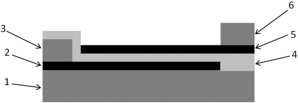
[0060] A graphene electro-optic modulator, its optical microscopic image is attached Figure 15 As shown, it includes an optical substrate 1, a bottom graphene 2, a lower metal electrode 3, an insulating layer 4, a top graphene 5 and an upper metal electrode 6 from bottom to top, and the top graphene 5 and the bottom graphene 2 are arranged oppositely, At the same time, there is no top-layer graphene 5 directly above the lower metal electrode 3, and no bottom-layer graphene directly below the upper metal electrode 6. The optical substrate 1 is a 2*2cm double-sided polished quartz sheet with a small insertion loss, and the top layer of graphite Both the graphene 5 and the bottom graphene 2 are made of single-layer graphene, and the single-layer graphene is grown on the copper foil substrate by chemical vapor deposition, and the lower metal electrode 3 and the upper metal electrode 6 are both Ti / Au with a thickness of 5 / 50nm. The distance between the two electrodes is 500 μm. T...
PUM
| Property | Measurement | Unit |
|---|---|---|
| thickness | aaaaa | aaaaa |
| thickness | aaaaa | aaaaa |
| thickness | aaaaa | aaaaa |
Abstract
Description
Claims
Application Information


