Optical fingerprint recognition device and forming method thereof

A fingerprint identification and optical technology, applied in the field of image processing, can solve the problems of long optical path, low output, inability to apply portable electronic devices, etc., and achieve the effect of reducing costs

Active Publication Date: 2016-08-17
GALAXYCORE SHANGHAI
View PDF10 Cites 4 Cited by
  • Summary
  • Abstract
  • Description
  • Claims
  • Application Information

AI Technical Summary

Problems solved by technology

[0004] However, the current optical fingerprint identification devices are large in size and have a long optical path, so they cannot be applied to portable electronic devices such as mobile phones
Under the premise of limited volume, the fingerprint recognition device suitable for portable electronic devices such as mobile phones needs to use a lens with a finer and more complex three-dimensional surface to ensure the required optical properties, such as resolution. However, using traditional micro-processing technology, For example, anisotropic or isotropic dry etching and wet etching can only process surfaces with limited topography, and newly developed three-dimensional micromachining technologies such as multi-layer mask technology, laser three-dimensional lithography, and electron beam direct writing technology , there are problems such as poor accuracy, high cost, and low output, which cannot meet the production requirements of such high-precision devices.

Method used


Image

  • Optical fingerprint recognition device and forming method thereof
  • Optical fingerprint recognition device and forming method thereof
  • Optical fingerprint recognition device and forming method thereof

Examples


Embodiment 1

[0027] Figure 1-Figure 10 It is a schematic diagram of the process of forming the optical fingerprint identification device according to Embodiment 1 of the present invention.

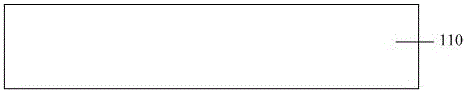
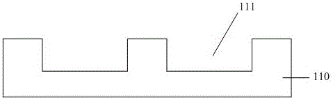
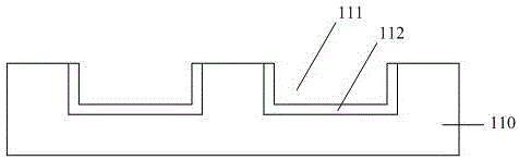
[0028] Such as Figure 1-Figure 3 As shown, a silicon substrate 110 is provided, and a groove array 111 is formed on the silicon substrate 110 . Preferably, a silicon dioxide layer, silicon nitride layer or titanium layer 112 is formed on the groove array 111 as a stop layer for subsequent etching.

[0029] Such as Figure 4-Figure 6 As shown, a light-transmitting substrate 120 and an image sensor chip 130 are provided. After bonding the light-transmitting substrate 120 and the image sensor chip 130, the backside of the image sensor chip 130 is thinned, and then the light-transmitting substrate 120 is formed on the light-transmitting substrate 120 by a gradual light flux lithography method. A lens array 150 corresponding to a photosensitive array (not shown) of the image sensor chip 130 is formed. ...

Embodiment 2

[0034] Figure 11-Figure 18 It is a schematic diagram of the process of the forming method of the optical fingerprint identification device according to the second embodiment of the present invention.

[0035] Such as Figure 11 As shown, a silicon substrate 210 is provided. Preferably, a silicon dioxide layer, a silicon nitride layer or a titanium layer 211 is formed on the silicon substrate 210 as a stop layer for subsequent etching.

[0036] Such as Figure 12-Figure 14 As shown, a light-transmitting substrate 220 and an image sensor chip 230 are provided. After bonding the light-transmitting substrate 220 and the image sensor chip 230, the backside of the image sensor chip 230 is thinned, and then the light-transmitting substrate 220 is formed on the light-transmitting substrate 220 by a gradual light flux lithography method. A lens array 250 corresponding to a photosensitive array (not shown) of the image sensor chip 230 is formed. Preferably, the protective film 251 i...


PUM


Abstract

The invention provides an optical fingerprint recognition device and a forming method thereof. A lens array is formed through a gradually-changing luminous flux photoetching method so that requirements for manufacturing of a more exquisite and complex lens can be met, optical characters needed by the optical fingerprint recognition device are accurately guaranteed, and the optical fingerprint recognition device and the forming method thereof are suitable for a portable electronic device and are compatible with an existing chip manufacturing and packaging technology so that cost can be reduced.

Description

technical field [0001] The invention relates to the field of image processing, in particular to an optical fingerprint recognition device and a forming method thereof. Background technique [0002] The current fingerprint identification schemes include optical technology, silicon technology (capacitive / radio frequency type), ultrasonic technology, etc. [0003] Optical technology The use of optical imaging equipment is based on the principle of total reflection of light (FTIR). The light hits the surface of the glass with fingerprints, and the reflected light is obtained by the image sensor. The amount of reflected light depends on the depth of the fingerprint ridges and valleys pressed on the surface of the glass, as well as the oil and moisture between the skin and the glass. After the light is shot to the center of the valley through the glass, it is totally reflected at the interface between the glass and the air, and the light is reflected to the image sensor, while th...

Claims


Application Information

Patent Timeline
Patent Type & Authority Applications(China)
IPC IPC(8): G06K9/00
CPCG06V40/1318
Inventor 赵立新陈俭夏欢
Owner GALAXYCORE SHANGHAI
Why Eureka
Try Eureka