
Two-dimensional electrode of crystalline silicon solar cell and preparation method of two-dimensional electrode

A technology of solar cells and crystalline silicon cells, which is applied in the field of solar cells, can solve the problems of limited reduction of electrode light-shielding area, complicated process, and inability to realize mass production, etc., and achieve good local ohmic contact, increase of light-receiving area, and balance dilemma problem effect

Active Publication Date: 2016-08-17
LERRI SOLAR TECH CO LTD
View PDF5 Cites 7 Cited by
  • Summary
  • Abstract
  • Description
  • Claims
  • Application Information

AI Technical Summary

Problems solved by technology

Some people propose to use a transparent conductive film to replace the metal fine grid, but because this method still retains the main grid, the reduction of the light-shielding area of ​​the electrode is limited, and the cancellation of the thin grid will cause poor conductivity and affect the conversion efficiency.
Some people use transparent conductive films with different conductivity to completely replace the metal electrodes and anti-reflection films on the light-receiving surface, but this method has not been mass-produced for more than ten years since it was proposed.
Some people apply transparent conductive film to MWT technology, but the implementation process is complicated, and it is not easy to control and reduce costs

Method used


Image

  • Two-dimensional electrode of crystalline silicon solar cell and preparation method of two-dimensional electrode
  • Two-dimensional electrode of crystalline silicon solar cell and preparation method of two-dimensional electrode
  • Two-dimensional electrode of crystalline silicon solar cell and preparation method of two-dimensional electrode

Examples


preparation example Construction

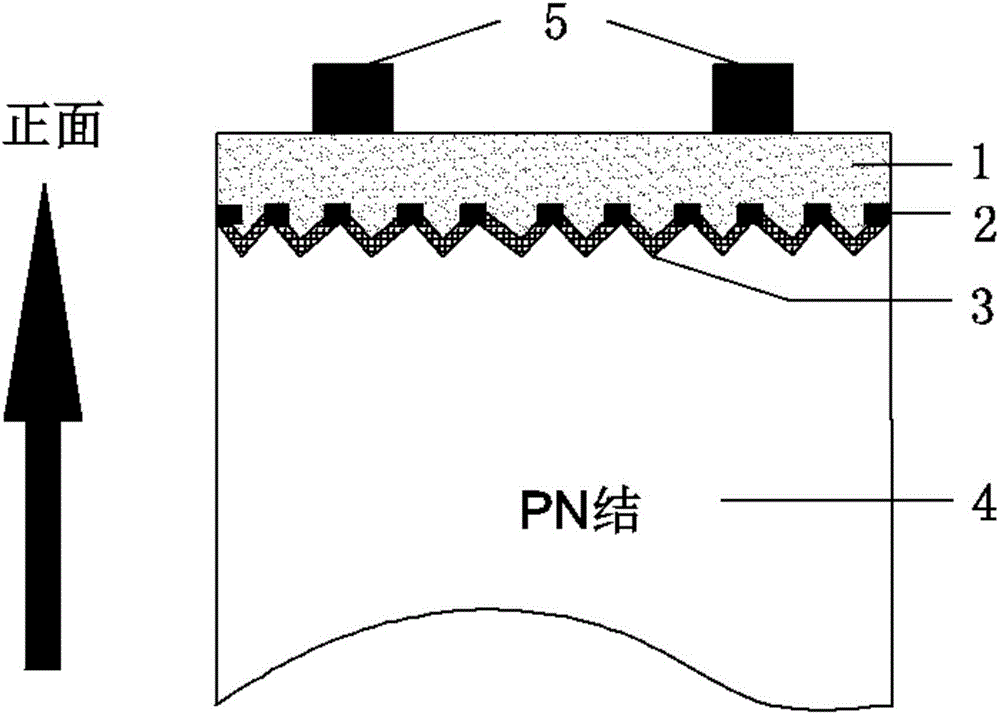
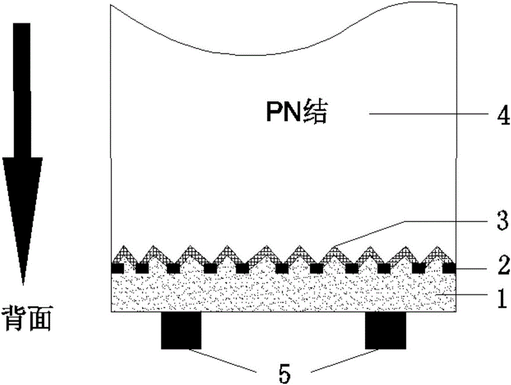
[0035] The method for preparing the two-dimensional electrode of the above-mentioned crystalline silicon solar cell comprises the following steps:

[0036] The crystalline silicon wafer 4 is processed through processes such as texturing, diffusion, etching, deposition of passivation film and anti-reflection film 3, etc. The crystalline silicon wafer 4 can be a P-type or N-type single crystal silicon wafer or polycrystalline silicon wafer, and then the crystalline silicon battery The electrodes are fabricated according to the following steps.

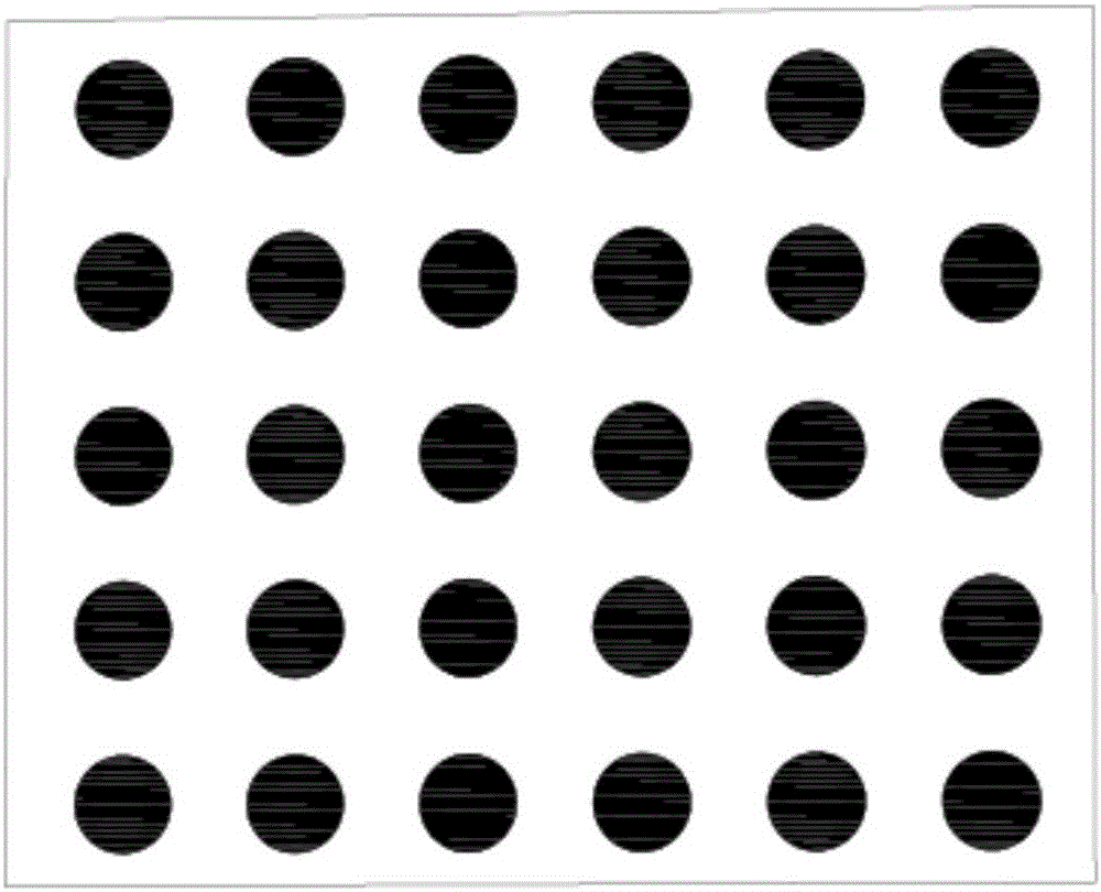
[0037] According to a specific pattern, on the front and / or back of the crystalline silicon cell, the local contact metal electrodes 2 distributed in an array that are in local contact with the silicon substrate can be made. The method of silk screen printing, laser or chemical corrosion can be used to cooperate with vapor deposition, photoelectric Methods of induction plating, electroplating, etc. Metal electrode patterns can be one-dime...

Embodiment 1

[0045] (1) P-type monocrystalline silicon wafers are processed through processes such as texturing, diffusion, etching, deposition of passivation film and anti-reflection film;

[0046] (2) adopt screen printing method to make dotted silver electrode on the front, the diameter of single dot is 50um, and the distance between dot and dot is 0.8mm;

[0047] (3) Carry out sintering at 300-900°C in the furnace body, and the dotted silver paste on the front side penetrates the anti-reflection film and passivation film to form a good ohmic contact with the silicon substrate;

[0048] (4) adopt the sputtering method to prepare the AZO transparent conductive film of 100nm on the dotted local contact silver electrode;

[0049] (5) Silver grid wire electrodes were prepared by screen printing on the AZO transparent conductive film. The electrode pattern consisted of a group of equidistant parallel grid lines, the number of grid lines was 20, and the width of the grid lines was 20um. Heat...

Embodiment 2

[0052] (1) P-type monocrystalline silicon wafers are processed through processes such as texturing, diffusion, etching, deposition of passivation film and anti-reflection film;

[0053] (2) Dot-shaped silver electrodes are made respectively by screen printing on the front and back, the diameter of a single dot is 100um, and the distance between dots is 1.5mm;

[0054] (3) Carry out sintering at 300-900°C in the furnace body, and the point-shaped silver paste on the front and back of the battery penetrates the anti-reflection film and passivation film, forming a good ohmic contact with the silicon substrate;

[0055] (4) Prepare a 110nm ITO transparent conductive film by sputtering on the point-like local contact electrode;

[0056] (5) On the ITO transparent conductive film, the silver electrode is prepared by inkjet method. The electrode pattern is composed of a group of equidistant parallel thin grid lines and a group of equidistant parallel busbar lines, and the thin grid l...


PUM

PropertyMeasurementUnit
Thicknessaaaaaaaaaa
Line widthaaaaaaaaaa
Lengthaaaaaaaaaa

Abstract

The invention discloses a two-dimensional electrode of a crystalline silicon solar cell and a preparation method of the two-dimensional electrode. The two-dimensional electrode is arranged on the front surface and / or the back surface of the crystalline silicon cell and comprises local contact metal electrodes, a transparent conductive film and metal electrodes, wherein the local contact metal electrodes are arranged on an antireflection film / passivating film in a regular pattern manner; the metal electrodes penetrate through the antireflection film / passivating film; the metal electrodes and a crystalline silicon wafer form local ohmic contact; the transparent conductive film is arranged on the antireflection film / passivating film and the local contact metal electrodes; the metal electrodes are arranged on the transparent conductive film; and the metal electrodes at the upper part and the lower part of the transparent conductive film are connected into a conductive assembly of the electrode of the crystalline silicon solar cell by the transparent conductive film. By the electrode, the light shading area of the metal electrodes and the usage amount of slurry are significantly reduced; meanwhile, good conductivity of the electrode is ensured; the dilemma between the light shielding property and the conductivity of the crystalline silicon electrode is well balanced; the conversion efficiency of the cell is improved; and the production cost is reduced.

Description

technical field [0001] The invention belongs to the technical field of solar cells, in particular to a two-dimensional electrode of a crystalline silicon solar cell and a preparation method thereof. Background technique [0002] Since the first solar cell was born in Bell Laboratories in 1954, crystalline silicon solar cells have been widely used, the conversion efficiency has been continuously improved, and the production cost has continued to decline. At present, crystalline silicon solar cells account for more than 80% of the total global solar cell market, and the conversion efficiency of crystalline silicon cell production lines has exceeded 20%. The cost of electricity continues to shrink and is expected to be flat in the next few years. As a clean energy source, crystalline silicon solar cells play an increasingly important role in changing the energy structure and alleviating environmental pressure. [0003] If crystalline silicon solar cells want to continue to ma...

Claims


Application Information

Patent Timeline
IPC IPC(8): H01L31/0224H01L31/068H01L31/18
CPCH01L31/022433H01L31/022466H01L31/068H01L31/1884Y02E10/547Y02P70/50
Inventor 钟宝申李华赵科雄
Owner LERRI SOLAR TECH CO LTD
Features
  • Generate Ideas
  • Intellectual Property
  • Life Sciences
  • Materials
  • Tech Scout
  • Unparalleled Data Quality
  • Higher Quality Content
  • 60% Fewer Hallucinations
Learn More