LED (light-emitting diode) epitaxial growth method capable of improving hole injection

A light-emitting diode, epitaxial growth technology

Active Publication Date: 2016-08-17
XIANGNENG HUALEI OPTOELECTRONICS
View PDF4 Cites 2 Cited by
  • Summary
  • Abstract
  • Description
  • Claims
  • Application Information

AI Technical Summary

Problems solved by technology

[0017] In view of this, the present invention provides a light-emitting diode epitaxial growth method that improves hole injection, which solves the shortcomings of low hole mobility, high LED operating voltage, and low luminous efficiency in traditional LED chips.

Method used


Image

  • LED (light-emitting diode) epitaxial growth method capable of improving hole injection
  • LED (light-emitting diode) epitaxial growth method capable of improving hole injection
  • LED (light-emitting diode) epitaxial growth method capable of improving hole injection

Examples


Embodiment 1

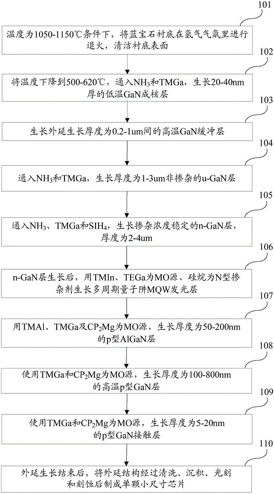
[0071] Such as image 3 As shown, is a schematic flow chart of an alternative embodiment of the epitaxial growth method of a light-emitting diode with improved hole injection according to the present invention. The invention grows Mg-doped and Mg-non-doped InGaN:Mg / InGaN superlattice layer structures in the LED epitaxial layer, improves the hole injection level of the quantum well region, reduces the working voltage of the light-emitting diode (LED) and improves the Luminous efficiency of LEDs. The light-emitting diode epitaxial growth method for improving hole injection described in this embodiment includes the following steps:

[0072] Step 301 , at a temperature of 1050-1150° C., anneal the sapphire substrate in a hydrogen atmosphere with a purity above 99.999%, and then clean the surface of the substrate.

[0073] Step 302, lower the temperature to 500-620°C, feed TMGa and NH with a purity of 99.999% or more 3 , grow a low-temperature GaN nucleation layer with a thickne...

Embodiment 2

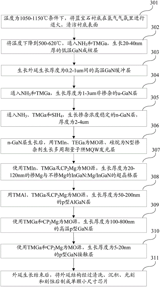
[0088] Such as Figure 5 As shown, it is a schematic flowchart of the epitaxial growth method of light-emitting diodes with improved hole injection described in Embodiment 2 of the present invention. In this embodiment, a specific method for realizing each step of epitaxial growth of a light emitting diode is provided. The light-emitting diode epitaxial growth method for improving hole injection in this embodiment includes the following steps:

[0089] Step 501 , after annealing the sapphire substrate in a hydrogen atmosphere with a purity above 99.999% at a temperature of 1050-1150° C., the surface of the substrate is cleaned.

[0090] Step 502, lower the temperature to 500-620°C, feed TMGa and NH with a purity of 99.999% or more 3 , under the condition that the growth pressure is 400-650 Torr and the V / III molar ratio is 500-3000, a low-temperature GaN nucleation layer with a thickness of 20-40 nm is grown.

[0091] Step 503, stop feeding TMGa, raise the temperature to 10...

Embodiment 3

[0105] In this embodiment, the LEDs prepared by the traditional method and the LEDs prepared by the solution of the present invention were used to conduct contrast tests of brightness and driving voltage. details as follows:

[0106] Sample 1 was prepared according to the traditional LED growth method, and sample 2 was prepared according to the method described in this patent; the difference between the parameters of the epitaxial growth method of sample 1 and sample 2 is that sample 2 was grown by the method of the present invention after the MQW light-emitting layer was grown. A layer of Mg-doped and non-Mg-doped InGaN:Mg / InGaN superlattice layer structure was prepared. For details, refer to sample 1 and sample 2 in Table 1. ITO (indium tin oxide, indium tin oxide, Commonly known as ITO) layer, 70nm Cr / Pt / Au electrodes are plated under the same conditions, and SiO is plated under the same conditions 2 The protective layer is 30nm, and then the sample is ground and cut into ...


PUM

PropertyMeasurementUnit
Thicknessaaaaaaaaaa
Thicknessaaaaaaaaaa
Thicknessaaaaaaaaaa

Abstract

The invention discloses an LED (light-emitting diode) epitaxial growth method capable of improving hole injection. The LED epitaxial growth method comprises the following steps: TMGa and NH3 are introduced and a low-temperature GaN nucleating layer grows after annealing of a sapphire substrate; a high-temperature GnA buffer layer epitaxially grows after in-situ annealing treatment is performed for 5-10 min; NH3 and TMGa are introduced, and a high-temperature non-doped u-GaN layer grows; NH3, TMGa and SiH4 are introduced, and a Si-doeped n-GaN layer grows; a MQW (multi-period quantum well) luminous layer grows; a Mg-doped and non-Mg-doped superlattice layer with the thickness of 20-120 nm grows; a p-type AlGaN layer grows; a p-type GnA layer grows; a p-type GaN contact layer grows; growth is ended after annealing treatment is performed in a nitrogen condition for 5-10 min; an obtained LED epitaxial structure is subjected to cleaning, deposition, photoetching and etching, and a single LED chip is prepared. The luminous efficiency of the LED is increased with the method.

Description

technical field [0001] The invention relates to the technical field of semiconductor chip fabrication, and more specifically, to an epitaxial growth method of a light-emitting diode that improves hole injection. Background technique [0002] Light-emitting diode (Light-Emitting Diode, referred to as LED) is a semiconductor electronic device that converts electrical energy into light energy. ), the working current is very small (some can emit light with only a few tenths of milliamperes), the impact resistance and shock resistance are good, the reliability is high, the service life is long, and the characteristics of easily modulating the intensity of light emission are very popular. With the vigorous development of the third-generation semiconductor technology, semiconductor lighting has become the focus of social development due to its advantages of energy saving, environmental protection, high brightness, and long life, and has also driven the development of the entire ind...

Claims


Application Information

Patent Timeline
IPC IPC(8): H01L33/00H01L33/06H01L33/12H01L33/14
CPCH01L33/0075H01L33/06H01L33/12H01L33/145H01L2933/0033
Inventor 林传强
Owner XIANGNENG HUALEI OPTOELECTRONICS
Why Eureka
Try Eureka