Inverted blue light quantum-dot thin film electroluminescence device and manufacturing method thereof

A technology for electroluminescent devices and quantum dots to emit light, which can be used in the manufacture of semiconductor/solid-state devices, electric solid-state devices, electrical components, etc., and can solve problems such as restricting and restricting luminous efficiency.

Inactive Publication Date: 2016-08-24
SHANGHAI UNIV
View PDF6 Cites 7 Cited by
  • Summary
  • Abstract
  • Description
  • Claims
  • Application Information

AI Technical Summary

Problems solved by technology

[0005] The QLEDs devices in the prior art have the following problems: the main problem of the QLED devices prepared by the core-shell structure CdSe@ZnS material is that the highest molecular orbital position (HOMO, Highest Occupied Molecular Orbital) of the QDs material itself is relatively high ( >6.0eV), especially for green and blue QDs, their HOMO energy levels are greater than 6.5eV, while the HOMO energy levels of commonly used hole transport materials are generally between 5.5eV and 6.0eV, which results in QLEDs devices The higher hole injection barrier restricts the process of direct carrier injection to form excitons. At the same time, QDs have a wide and continuous absorption spectrum that makes it easy to absorb external energy to form excitons. Therefore, the light-emitting excitons in QLEDs The formation of carriers is mainly affected by the joint action of two mechanisms: direct carrier injection and energy transfer.
The improvement of direct carrier injection will generally enhance the luminous efficiency of QLEDs devices; and the energy transfer mechanism is generally carried out from high energy gap materials to low energy gap materials. Therefore, for high energy gap blue light and green light, the energy transfer mechanism The occurrence of often restricts the improvement of its luminous efficiency

Method used


Image

  • Inverted blue light quantum-dot thin film electroluminescence device and manufacturing method thereof
  • Inverted blue light quantum-dot thin film electroluminescence device and manufacturing method thereof
  • Inverted blue light quantum-dot thin film electroluminescence device and manufacturing method thereof

Examples


Embodiment 1

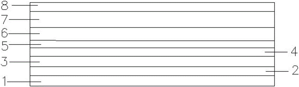
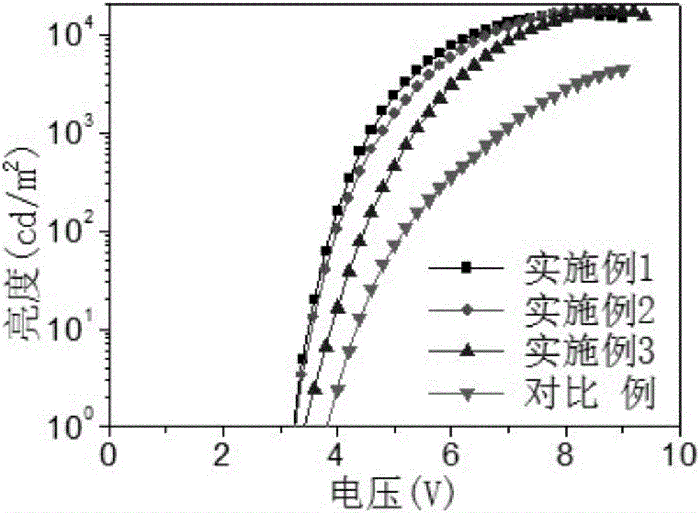
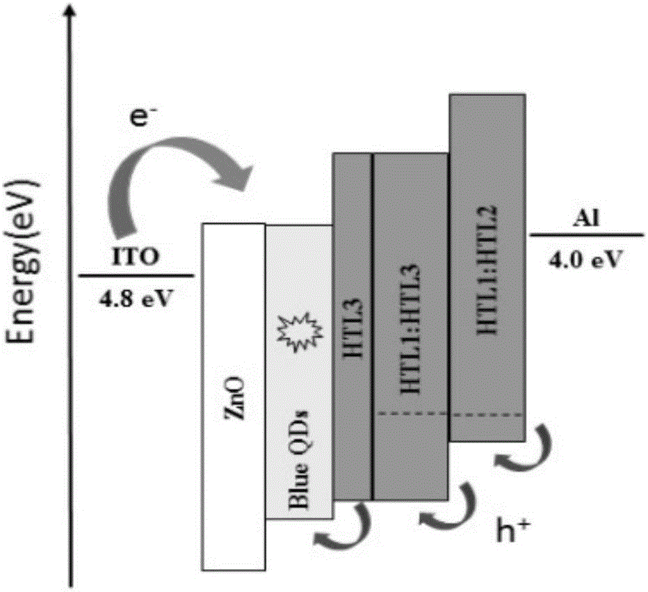
[0044] Substrate 1 was first ultrasonically treated with detergent, acetone, ethanol and isopropanol for 15 min each. Then a layer of ITO conductive film with a thickness of 150nm was sputtered on the substrate 1, and then UV-ozone was performed for 15 minutes. Next, the ZnO electron transport layer 3 was prepared in a glove box filled with nitrogen and extremely low in water and oxygen content by solution spin coating, using 20 mg / ml of ZnO nanoparticle ethanol solution at a speed of 1500 rpm (Resolutions per minute, rpm), Annealed at 150°C for 30min, with a thickness of 40nm. Then prepare the quantum dot light-emitting layer, using 20mg / ml blue CdSe@ZnS quantum dot toluene solution, rotating at 2000rpm, annealing at 150°C for 30min, with a thickness of 20nm. The device was then transferred to a pressure of 10 -4 In the high vacuum chamber under Pa, 8nm BCPPA is vacuum-evaporated sequentially as the third hole transport layer; the 15nm doping material is MoO with a mass rat...

Embodiment 2

[0046] Substrate 1 was first ultrasonically treated with detergent, acetone, ethanol and isopropanol for 15 min each. Then a layer of ITO conductive film with a thickness of 150nm was sputtered on the substrate 1, and then UV-ozone was performed for 15 minutes. Next, the ZnO electron transport layer 3 was prepared in a glove box filled with nitrogen and extremely low in water and oxygen content by solution spin coating, using 20 mg / ml of ZnO nanoparticle ethanol solution at a speed of 1500 rpm (Resolutions per minute, rpm), Annealed at 150°C for 30min, with a thickness of 40nm. Then prepare the quantum dot light-emitting layer, using 20mg / ml blue CdSe@ZnS quantum dot toluene solution, rotating at 2000rpm, annealing at 150°C for 30min, with a thickness of 20nm. The device was then transferred to a pressure of 10 -4 In the high vacuum chamber under Pa, 8nm BCPPA is vacuum-evaporated sequentially as the third hole transport layer; the 20nm doping material is MoO with a mass rat...

Embodiment 3

[0048]Substrate 1 was first ultrasonically treated with detergent, acetone, ethanol and isopropanol for 15 min each. Then sputter a layer of ITO conductive film with a thickness of 200nm on the substrate, and then perform UV-ozone treatment for 15min. Next, the ZnO electron transport layer 3 was prepared in a glove box filled with nitrogen and extremely low in water and oxygen content by solution spin coating, using 20 mg / ml of ZnO nanoparticle ethanol solution at a speed of 1500 rpm (Resolutions per minute, rpm), Annealed at 150°C for 30min, with a thickness of 40nm. Then prepare the quantum dot light-emitting layer, using 20mg / ml blue CdSe@ZnS quantum dot toluene solution, rotating at 2000rpm, annealing at 150°C for 30min, with a thickness of 20nm. The device was then transferred to a pressure of 10 -4 In the high vacuum chamber under Pa, 10nm BCPPA is vacuum-evaporated sequentially as the third hole transport layer; the 20nm doping material is MoO with a mass ratio of 1:4...


PUM


Abstract

An inverted blue light quantum-dot thin film electroluminescence device disclosed by the present invention comprises a substrate, a cathode, an electronic transmission layer, a blue light quantum-dot luminescent layer, hole transport layers and an anode which are laminated orderly, and the hole transport layers comprise a third hole transport layer, a second hole transport layer and a first hole transport layer which are laminated orderly. The thickness of the third hole transport layer is between 5 nm and 10 nm, and the HOMO energy level of the second hole transport layer is greater than the HOMO energy level of the first hole transport layer, thereby forming the ladder-like potential barrier between the blue light quantum-dot luminescent layer and the anode, improving the hole-injection ability of the hole transport layers gradually, and satisfying the hole injection requirement of the blue light quantum-dot thin film electroluminescence device. The electroluminescence device of the present invention is low in hole injection barrier and high in carrier direct injection mechanism and luminous efficiency. The present invention also provides a method for preparing the above inverted blue light quantum-dot thin film electroluminescence device.

Description

technical field [0001] The invention relates to the technical field of electroluminescent devices, in particular to an inverted blue light quantum dot thin film electroluminescent device and a manufacturing method thereof. Background technique [0002] Semiconductor quantum dots (QDs, Quantum Dots) materials with a diameter between 2nm and 10nm belong to quasi-zero-dimensional nanomaterials, also known as nanocrystals. Since electrons, holes, and excitons are quantum-confined in the three-dimensional direction, the energy band structure of QDs changes from a bulk continuous structure to a discrete energy level structure with molecular characteristics. When the radius is equal or smaller, the localization and coherence of electrons are enhanced, the absorption coefficient of the exciton band increases, strong absorption of excitons occurs, strong fluorescence can be emitted after excitation, and it has a narrow and symmetrical emission spectrum, wide and continuous Absorptio...

Claims


Application Information

Patent Timeline
Patent Type & Authority Applications(China)
IPC IPC(8): H01L51/50H01L51/56B82Y40/00
CPCB82Y40/00H10K50/155H10K50/156H10K71/00
Inventor 曹进周洁谢婧薇魏翔俞浩健
Owner SHANGHAI UNIV
Why Eureka
Try Eureka