A light-emitting diode epitaxial wafer and its preparation method

A technology of light-emitting diodes and epitaxial wafers, applied in semiconductor devices, electrical components, circuits, etc., can solve the problems of poor substrate adhesion and high cost, and achieve the effect of improving the peeling yield

Active Publication Date: 2018-10-02
ELEC TECH OPTOELECTRONICS TECHWUHUCO
View PDF6 Cites 0 Cited by
  • Summary
  • Abstract
  • Description
  • Claims
  • Application Information

AI Technical Summary

Problems solved by technology

The first method is limited to the use of silicon carbide as the growth substrate of GaN-based epitaxial wafers. Compared with the sapphire substrate used in large quantities today, it has the problem of high cost, while the second method uses the transfer method to place the graphene layer on the substrate. method, since the graphene layer itself is a two-dimensional material, it is easy to have poor adhesion to the substrate

Method used


Image

  • A light-emitting diode epitaxial wafer and its preparation method
  • A light-emitting diode epitaxial wafer and its preparation method
  • A light-emitting diode epitaxial wafer and its preparation method

Examples


Embodiment 1

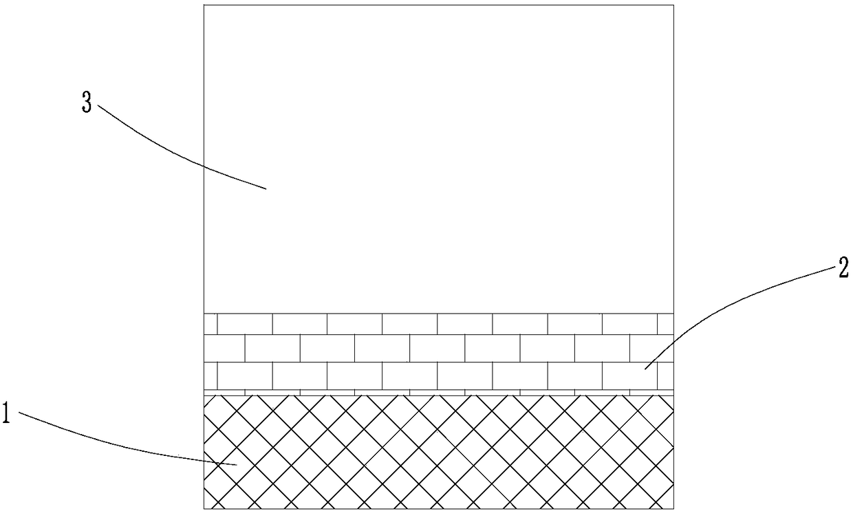
[0034] Such as figure 1 As shown, the traditional gallium nitride-based epitaxial wafer includes a buffer layer 2 and an epitaxial structure layer 3 from the substrate 1 to the surface layer. If the epitaxial structure layer 3 is to be stripped, a laser device must be used, and the stripping yield is not good.

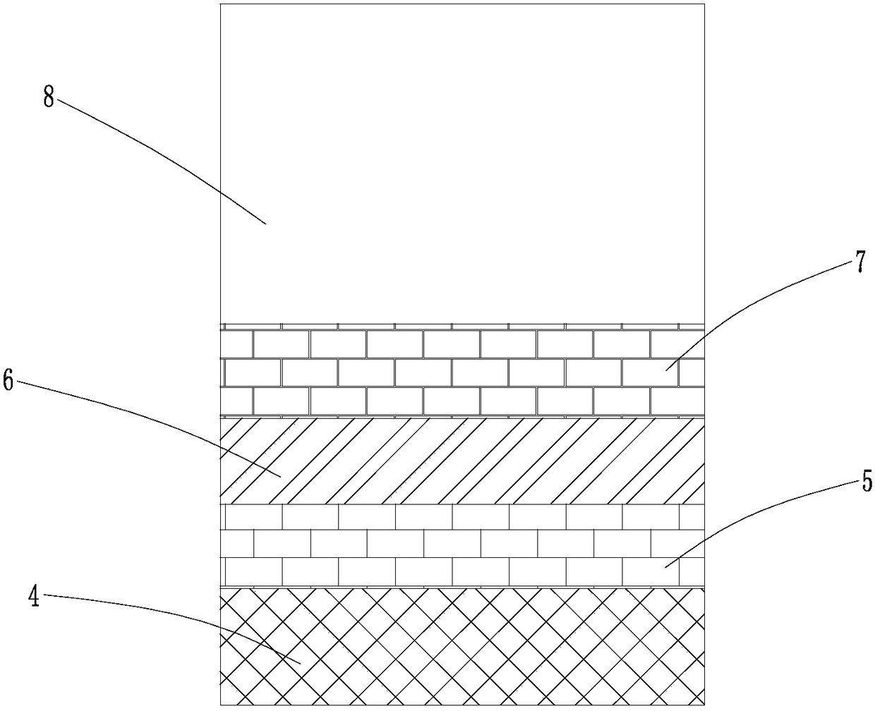
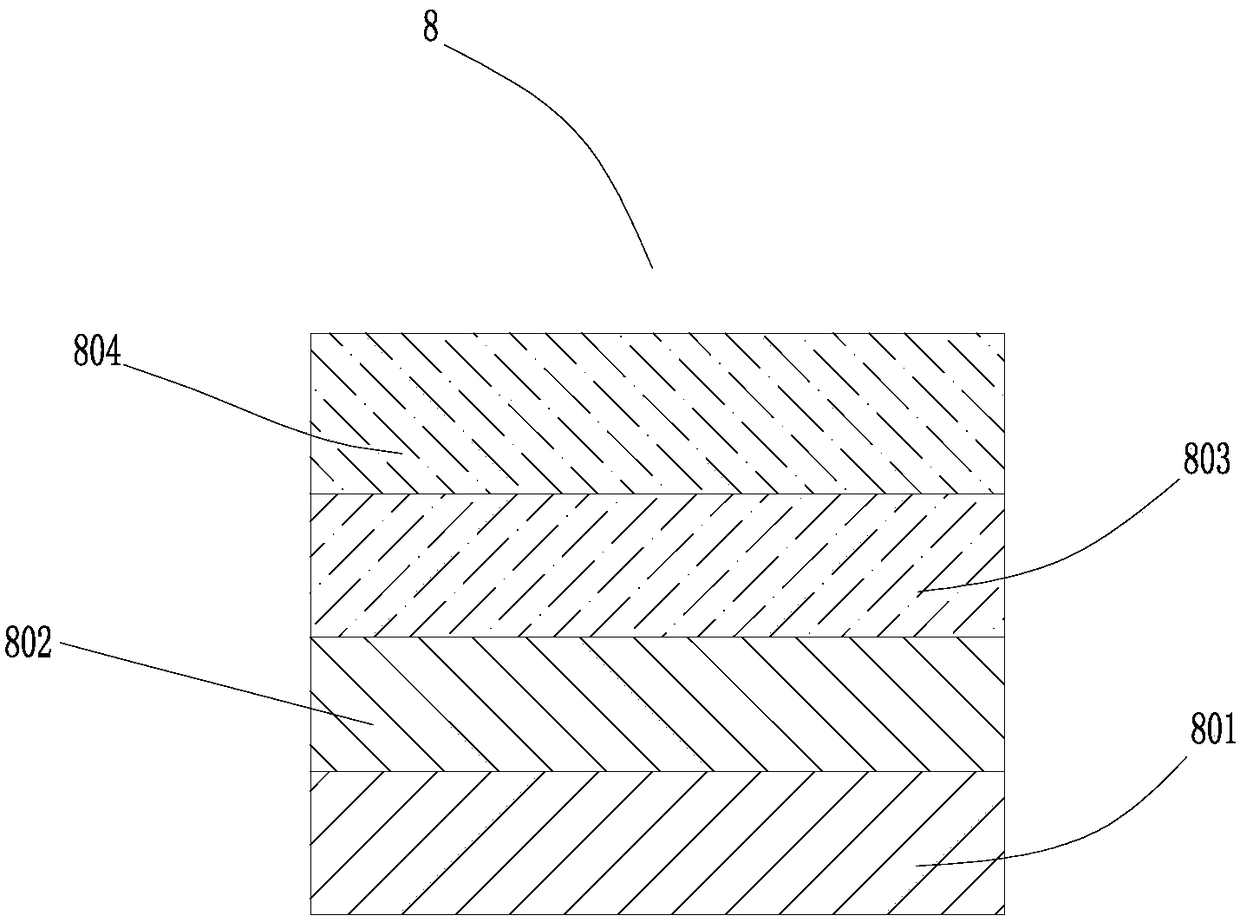
[0035] Such as figure 2 , image 3 As shown, the light-emitting diode epitaxial wafer of the present application, the epitaxial wafer includes a first buffer layer 5, a graphene layer 6, a second buffer layer 7 and an epitaxial structure layer 8 from the substrate 4 to the surface layer; the epitaxial structure layer 8 is formed from the second buffer layer 7 The surface layer is composed of an N-type semiconductor layer 801 , a multiple quantum well layer 802 , a P-type electron blocking layer 803 and a P-type semiconductor layer 804 .

[0036] The substrate 4 is a sapphire substrate.

[0037] The first buffer layer is SiCN with a thickness of 30-40nm; the composi...

Embodiment 2

[0046] The difference between embodiment 2 and embodiment 1 is: the difference of preparation method

[0047] 1) At a temperature of 1200°C, feed carbon source (CBr4), silicon source (SiH4) and nitrogen source (NH3) into the reaction chamber, and grow 30nm SiCN on the sapphire substrate as the first buffer layer; the first buffer layer The silicon content on the side close to the sapphire substrate is controlled below 10%, while the silicon content on the other side is greater than 30%;

[0048]2) At a temperature of 1200°C, feed carbon source (CBr4) and silicon source (SiH4) to grow 8nm silicon carbide on the first buffer layer; after that

[0049] At a temperature of 1500°C and a pressure of <1 Torr, silicon atoms are volatilized to form a graphene layer;

[0050] 3) At a temperature of 1000°C, feed carbon source (CBr4), silicon source (SiH4) and nitrogen source (NH3) into the reaction chamber, and grow a layer of SiCN on the graphene layer as the second buffer layer; or at...

Embodiment 3

[0053] The difference between embodiment 3 and embodiment 1 is; the difference of preparation method

[0054] 1) At a temperature of 850°C, feed carbon source (CBr4), silicon source (SiH4) and nitrogen source (NH3) into the reaction chamber, and grow 35nm SiCN on the sapphire substrate as the first buffer layer; the first buffer layer The silicon content on the side close to the sapphire substrate is controlled below 10%, while the silicon content on the other side is greater than 30%;

[0055] 2) At a temperature of 850°C, feed carbon source (CBr4) and silicon source (SiH4) to grow 12nm silicon carbide on the first buffer layer; then

[0056] At a temperature of 1400°C and a pressure of <1 Torr, silicon atoms are volatilized to form a graphene layer;

[0057] 3) At a temperature of 750°C, feed carbon source (CBr4), silicon source (SiH4) and nitrogen source (NH3) into the reaction chamber, and grow a layer of SiCN on the graphene layer as the second buffer layer; or at temper...


PUM


Abstract

The invention discloses a light-emitting diode epitaxial wafer and a preparation method thereof, which belong to the photoelectric field. The epitaxial wafer comprises a first buffer layer, a graphene layer, a second buffer layer and an epitaxial structure layer from a substrate to a surface layer; and the epitaxial structure layer is composed of an N-type semiconductor layer, a multiple quantum well layer, a P-type electron blocking layer and a P-type semiconductor layer from the second buffer layer to the surface layer. In comparison with the traditional GaN-based epitaxial wafer structure, the graphene layer is added to enable the GaN-based epitaxial structure layer to be stripped from the substrate by using a mechanical mode, a laser device does not need to be adopted, and the stripping yield is improved; in comparison with other techniques of using a transfer mode to place the graphene layer on the substrate, the buffer layers exist between the graphene layer and the substrate for connection, and the problem of poor adhesion between the graphene layer and the substrate does not exist.

Description

technical field [0001] The invention relates to the field of optoelectronics, in particular to a gallium nitride-based light-emitting diode epitaxial wafer with a graphene layer and a preparation method thereof. Background technique [0002] Graphene is a two-dimensional material composed of one or more layers. It is applied on GaN-based epitaxial wafers. Since the graphene layer and the nitride epitaxial layer form molecular bonds with weaker bond energy at the interface connection, this makes graphite The lift-off between the olefin layer and the nitride epitaxial layer provides feasibility. [0003] There are generally two ways to apply graphene to the structure of gallium nitride-based epitaxial wafers. One is to use a silicon carbide substrate to sublimate silicon atoms at a high temperature of about 1500 ° C to complete graphitization; the other is to use graphene materials directly The transfer is placed on the substrate of the gallium nitride-based epitaxial wafer, ...

Claims


Application Information

Patent Timeline
Patent Type & Authority Patents(China)
IPC IPC(8): H01L33/12H01L33/32H01L33/00
CPCH01L33/0075H01L33/12H01L33/32
Inventor 陈铭胜武良文
Owner ELEC TECH OPTOELECTRONICS TECHWUHUCO
Why Eureka
Try Eureka