Manufacturing method of N type/P type monocrystalline silicon crystal ingot

A manufacturing method and technology of single crystal silicon, which are applied in the directions of single crystal growth, single crystal growth, chemical instruments and methods, etc., can solve the problems of low utilization rate of doping gas, difficult doping elements, poor operability, etc.

Inactive Publication Date: 2016-09-21
SHANGHAI ADVANCED SILICON TECH CO LTD
View PDF10 Cites 6 Cited by
  • Summary
  • Abstract
  • Description
  • Claims
  • Application Information

AI Technical Summary

Problems solved by technology

However, in the gas phase doping process, the argon gas flow rate is fast, the flow rate is large, the utilization rate of the doping gas is low, and the doping elements are difficult to effectively integrate into the silicon melt, so the ability to control the axial resistivity fluctuation in the silicon ingot is limited.
Even when the doping concentration is high, it is difficult to uniformly dilute the phosphine with the inert gas, resulting in the inversion of the single crystal silicon due to the excessive concentration of the local doping gas in the Czochralski silicon single crystal.
Therefore, this method is only suitable for photovoltaic solar cells with low resistivity
In addition, phosphine gas is a toxic gas with extremely poor safety, high cost of use and disposal, and poor operability

Method used


Image

  • Manufacturing method of N type/P type monocrystalline silicon crystal ingot
  • Manufacturing method of N type/P type monocrystalline silicon crystal ingot
  • Manufacturing method of N type/P type monocrystalline silicon crystal ingot

Examples


Embodiment 1

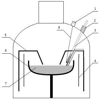
[0038] An 8-inch N-type monocrystalline silicon rod in the direction was grown by the Czochralski method. Add 120Kg of polysilicon raw material and main dopant element phosphorus into the quartz crucible, the initial concentration of phosphorus is 8E13atoms / cm 3 . Under the protection of inert gas (usually argon), turn on the heater and gradually increase the temperature to above 1420°C to completely melt the raw materials.

[0039] According to the conventional Czochralski method single crystal silicon growth process such as seeding, necking, shouldering, and shouldering, etc. enters the equal-diameter growth process. From a P-type monocrystalline silicon rod with a diameter of 300 mm and a resistivity of 0.3 Ω·cm, a single crystal silicon strip of 20 mm×20 mm×200 mm is cut along the diameter direction. Since the doping element boron has a concentration deviation along the crystal growth direction, but is uniformly distributed in the diameter direction, this sampling metho...

Embodiment 2

[0045] 8-inch P-type monocrystalline silicon rods in the direction were grown by the Czochralski method. Add 120kg of polysilicon raw material and boron into the quartz crucible, the initial concentration of boron is 1.78E14 atoms / cm 3 . Under the protection of inert gas (usually argon), turn on the heater and gradually increase the temperature to above 1420°C to completely melt the raw materials.

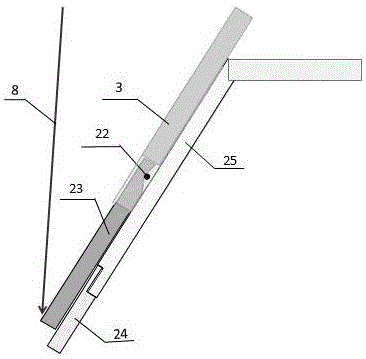
[0046] According to the conventional crystal growth parameters, seeding, shouldering, shoulder turning, and entering the equal-diameter stage are carried out. Cut out a 20mm×20mm×250mm monocrystalline silicon strip along the diameter direction from a phosphorus-doped monocrystalline silicon rod with a diameter of 300mm and a resistivity of 20Ω·cm, and fix it on a support as a source of secondary doping elements. When the solidification rate is 0.4, that is, when the crystal weight is 48kg, turn on the laser array, set the power to 50W, and melt a 0.46cm single crystal silicon st...


PUM

PropertyMeasurementUnit
electrical resistivityaaaaaaaaaa
wavelengthaaaaaaaaaa
electrical resistivityaaaaaaaaaa

Abstract

The invention provides a manufacturing method of an N type / P type monocrystalline silicon crystal ingot. During the lifting growth of the crystal ingot, monocrystalline silicon strips containing uniform distribution opposite type conducting elements (sub doping elements) are molten through laser arrays; the sub doping elements are added into the flux in a continuous and adjustable way; carriers increased in the crystal ingot due to the fast rise of the concentration of main doping elements in flux caused by dephlegmation are counteracted, so that the problem of fast reduction of the electrical resistivity in a late growth stage of the crystal ingot growth is solved. By precisely controlling the addition quantity and the addition speed of the sub doping elements, the carrier density in the crystal ingot in a new crystallization region is stabilized, so that the electrical resistivity of the new crystallization region is stabilized; the fluctuation amplitude of the axial electrical resistivity of the whole crystal ingot is reduced; the utilization rate of the crystal ingot and the electric performance of wafers are improved.

Description

technical field [0001] The invention relates to the field of semiconductor material crystal growth and element doping, in particular to a method for doping and crystal growth of boron and phosphorus co-doped high-resistance single crystal silicon. Background technique [0002] In recent years, with the development of very large scale integrated circuits, the application fields of power devices have become wider and wider. The main feature of power devices is high voltage resistance, and the resistance of the substrate has a great influence on the performance of the device. Therefore, the resistivity of the substrate is required to be high and the resistivity change small. Due to the lattice mismatch between doping elements and silicon elements, there is a segregation phenomenon during the growth of single crystal silicon, that is, the concentration of doping elements crystallized in the single crystal silicon ingot is lower than that in the melt (raw material), so that the d...

Claims


Application Information

Patent Timeline
Patent Type & Authority Applications(China)
IPC IPC(8): C30B15/04C30B15/20C30B29/06
CPCC30B15/04C30B15/20C30B29/06
Inventor 刘浦锋宋洪伟陈猛
Owner SHANGHAI ADVANCED SILICON TECH CO LTD
Why Eureka
Try Eureka