A kind of semiconductor device and its manufacturing method, electronic device

A manufacturing method and semiconductor technology, applied in semiconductor devices, semiconductor/solid-state device manufacturing, circuits, etc., can solve the problem of poor off-state characteristics of MOSFET devices, short-channel effect and leakage-induced barrier reduction, and device performance degradation, etc. The problem is to reduce the degradation of carrier mobility, reduce the channel electric field, and reduce the leakage current.

Active Publication Date: 2021-04-13
SEMICON MFG INT (SHANGHAI) CORP
View PDF3 Cites 0 Cited by
  • Summary
  • Abstract
  • Description
  • Claims
  • Application Information

AI Technical Summary

Problems solved by technology

For example, as the channel size continues to decrease, the short channel effect and the drain-induced barrier lowering (DIBL) effect are becoming more and more serious, resulting in poor device performance.
At the same time, the leakage-induced barrier lowering (DIBL) effect will affect the sub-threshold characteristics, such as degrading the sub-threshold swing (or S factor). In the scaling rules of large-scale digital integrated circuits, the constant voltage scaling rule , the constant electric field reduction rule, etc. cannot reduce the S value, and the leakage current in the subthreshold region deteriorates the off-state characteristics of the MOSFET device and increases the static power consumption

Method used


Image

  • A kind of semiconductor device and its manufacturing method, electronic device
  • A kind of semiconductor device and its manufacturing method, electronic device
  • A kind of semiconductor device and its manufacturing method, electronic device

Examples


Embodiment 1

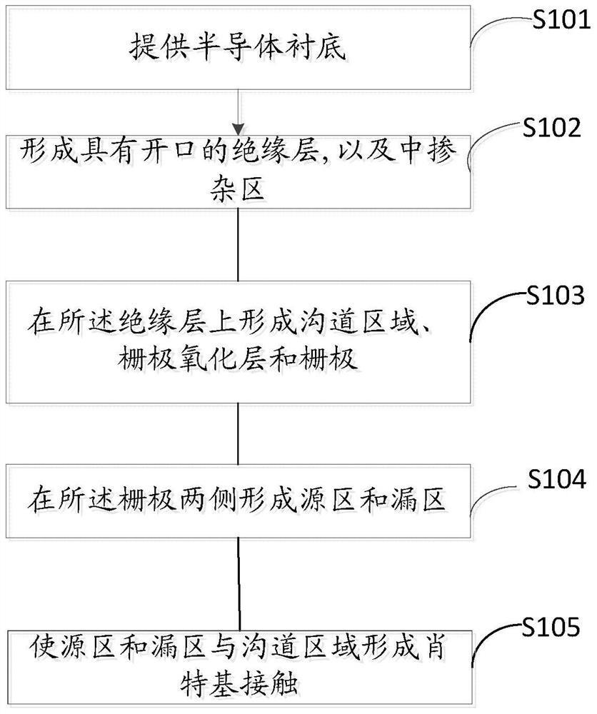
[0046] Figure 2a - Figure 2m A cross-sectional view of a device obtained at each step in a process flow for fabricating a semiconductor device according to an embodiment of the present invention. The following will refer to Figure 2a - Figure 2m The manufacturing method of the semiconductor device of the present invention will be described in detail.

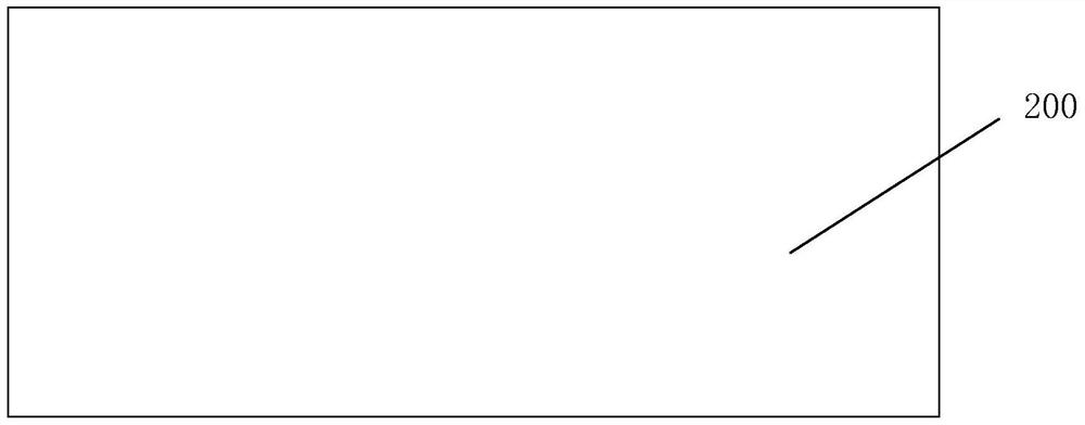
[0047] First, as Figure 2a As shown, a semiconductor substrate 200 is provided. The semiconductor substrate 200 may be at least one of the materials mentioned below: silicon, germanium, silicon germanium, and the like. In addition, other devices, such as PMOS and NMOS transistors, may be formed on the semiconductor substrate. An isolation structure may be formed in the semiconductor substrate, and the isolation structure may be a shallow trench isolation (STI) structure or a localized silicon oxide (LOCOS) isolation structure. CMOS devices, such as transistors (eg, NMOS and / or PMOS), etc., may also be formed in the semic...

Embodiment 2

[0076] The present invention also provides a semiconductor device 300 fabricated by the method described in Embodiment 1, comprising: a semiconductor substrate 200, an insulating layer 201 having an opening formed on the semiconductor substrate 200, a silicon layer located in the opening, and The channel region 211, the gate oxide layer 212 and the gate electrode 218 are located above the opening, and the source electrode 217A and the drain electrode 217B are located on both sides of the gate electrode 218; wherein, the surface layer of the semiconductor substrate in the opening and under the opening is formed The heavily doped region 204 ; the source 217A and the drain 217B form Schottky contacts with the channel region 211 .

[0077] Optionally, the source electrode 217A and the drain electrode 217B are formed with silicide.

[0078] Optionally, the insulating layer 201 is a silicon dioxide layer.

[0079] Optionally, the channel region 211 is an undoped layer or a lightly ...

Embodiment 3

[0084] The present invention further provides an electronic device including the aforementioned semiconductor device. Figure 4 It is a schematic structural diagram of an electronic device according to an embodiment of the present invention. Due to the inclusion of the aforementioned semiconductor device, the self-heating effect, the leakage-induced barrier lowering effect, and the sub-threshold characteristics of the device can be improved, and the electronic device also has the above-mentioned advantages.


PUM


Abstract

The present invention provides a method for manufacturing a semiconductor device, the method comprising: step a: providing a semiconductor substrate; step b: forming an insulating layer having an opening and a silicon layer located in the opening on the semiconductor substrate; Forming a heavily doped region in the opening region and the surface layer of the semiconductor substrate below the opening region; step c: forming a channel region, a gate oxide layer and a gate on the insulating layer; step d: forming a gate on the gate A source region and a drain region are formed on both sides; wherein, the source region and the drain region form a Schottky contact with the channel region. Through the manufacturing method of the semiconductor device of the invention, the self-heating effect, leakage-induced potential barrier lowering effect and subthreshold characteristics of the device can be improved.

Description

technical field [0001] The present invention relates to the technical field of semiconductors, and in particular, to a semiconductor device, a manufacturing method thereof, and an electronic device. Background technique [0002] In the contemporary information society, under the dual drive of maximizing chip integration density and optimizing circuit performance, the core MOSFET devices of integrated circuits are constantly being scaled down. Since the 1970s, due to the development of the ion implantation process, extremely small MOSFETs have been fabricated, and the theory of MOSFET scaling has been established. As the size of MOSFET devices continues to shrink, various small-size effects are gradually revealed. For example, as the channel size continues to decrease, the short-channel effect and the drain-induced barrier lowering (DIBL) effect become increasingly severe, resulting in poor device performance. At the same time, the leakage induced barrier lowering (DIBL) ef...

Claims


Application Information

Patent Timeline
Patent Type & Authority Patents(China)
IPC IPC(8): H01L21/336H01L29/78H01L29/06
Inventor 刘金华
Owner SEMICON MFG INT (SHANGHAI) CORP
Why Eureka
Try Eureka