

Method of preparing ESD device, and ESD device
A technology of ESD devices and epitaxial layers, which is applied in the manufacture of electric solid-state devices, semiconductor devices, semiconductor/solid-state devices, etc., can solve the effect of reducing the leakage induction barrier, increase the leakage current of device leakage junction capacitance, and reduce the performance of semiconductor devices, etc. question
- Summary
- Abstract
- Description
- Claims
- Application Information
AI Technical Summary
Problems solved by technology
Method used
Image

Examples
Embodiment 1
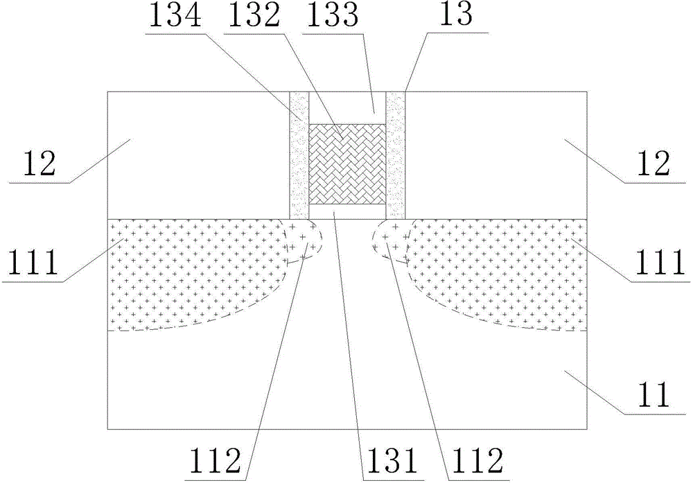
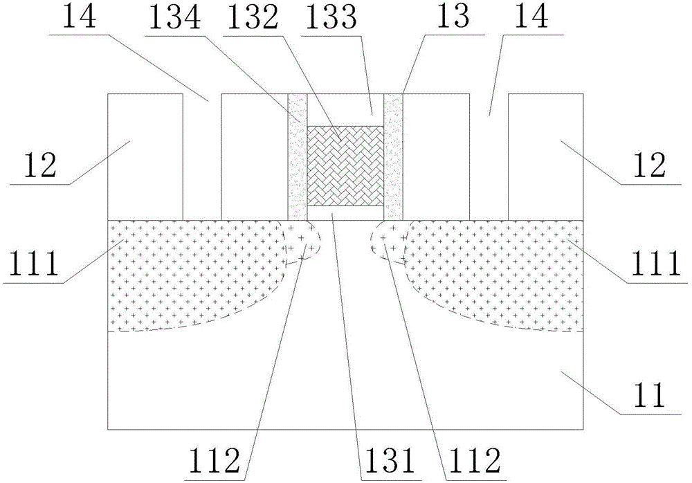
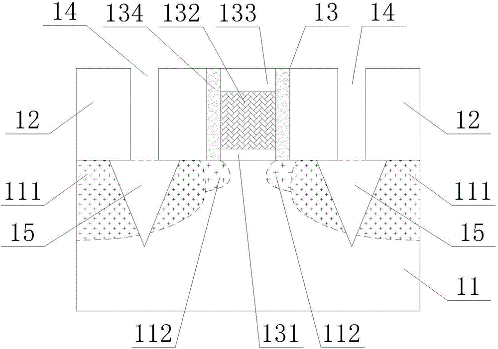
[0041] Figure 1~5 It is a schematic flow chart of the method for preparing an ESD device in Example 1 of the present application; as Figure 1~5 As shown, this embodiment is based on the preparation process of ESD devices based on the traditional preparation of MOS devices, specifically:
[0042] Such as figure 1 As shown, a silicon substrate 11 prepared with a well region is provided, and a gate stack structure 13 (gate stack after well) is prepared on the silicon substrate 11; the gate stack structure 13 can be prepared based on a traditional MOS device The high-k metal gate structure (HKMG) prepared by the process includes a gate oxide layer 131, a metal gate 132, a low resistance layer 133 and sidewalls 134, and the gate oxide layer 131 covers part of the upper surface of the silicon substrate 11, and the metal The gate 132 covers the upper surface of the gate oxide layer 131, the low-resistance layer 133 covers the upper surface of the metal gate 132, and the spacer 134...
Embodiment 2
[0051] Figure 6 It is a structural schematic diagram of an ESD device in Embodiment 2 of the present application; on the basis of the method for preparing an ESD device in Embodiment 1 above, the ESD device in this embodiment can be formed, specifically:
[0052] Such as figure 2 As shown, on the silicon substrate 21 forming the source / drain region 211, a gate stack structure 22 is provided, and the gate stack structure 22 may be a high-k metal gate structure (HKMG ), which specifically includes a gate oxide layer 221, a metal gate 222, a low-resistance layer 223, and sidewalls 224, and the gate oxide layer 221 covers part of the upper surface of the silicon substrate 21, and the metal gate 222 covers the upper surface of the gate oxide layer 221. On the surface, the low-resistance layer 223 covers the upper surface of the metal gate 222, the sidewall 224 is located on the upper surface of the silicon substrate 21 and covers the sidewalls of the gate oxide layer 221, the me...
PUM
| Property | Measurement | Unit |
|---|---|---|
| Depth | aaaaa | aaaaa |
Abstract
Description
Claims
Application Information