Epitaxial wafer of light-emitting diode and growing method thereof
A technology of light-emitting diodes and growth methods, which is applied in the field of epitaxial wafers of light-emitting diodes and their growth, can solve problems such as excessive local current and device failure, improve antistatic ability, improve expansion ability, and improve the problem of excessive local current Effect
- Summary
- Abstract
- Description
- Claims
- Application Information
AI Technical Summary
Problems solved by technology
Method used
Image

Examples
Embodiment 1
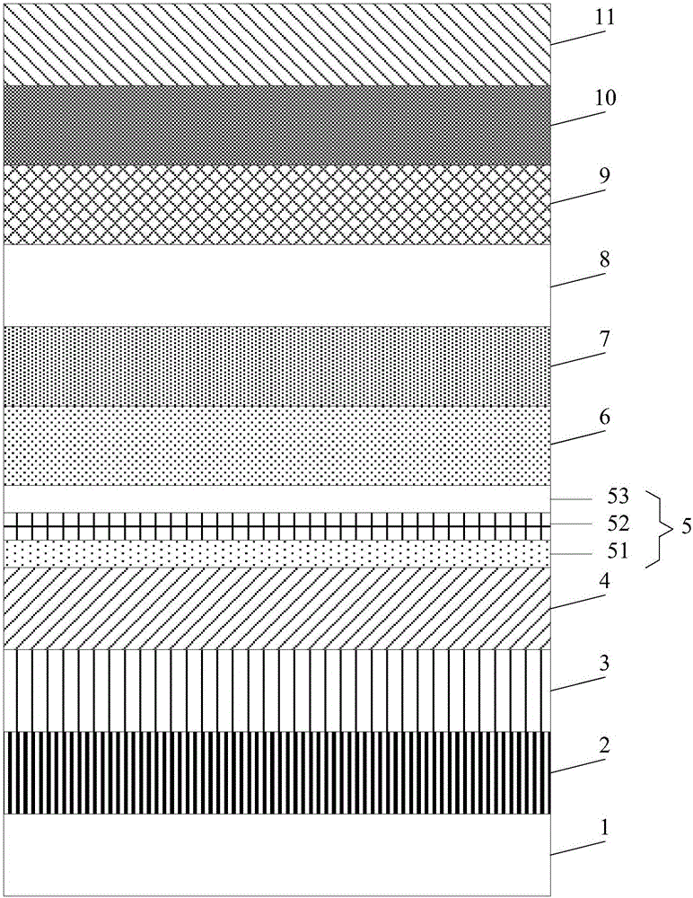
[0032] An embodiment of the present invention provides an epitaxial wafer of a light emitting diode, see figure 1 , the epitaxial wafer includes a sapphire substrate 1, and a buffer layer 2, an undoped GaN layer 3, an N-type GaN layer 4, a current spreading layer 5, a shallow well layer 6, and a multi-quantum well stacked sequentially on the sapphire substrate 1 layer 7, low-temperature P-type GaN layer 8, P-type electron blocking layer 9, high-temperature P-type GaN layer 10, and P-type contact layer 11.
[0033] In this embodiment, the current spreading layer 5 includes an AlN layer 51 , an InGaN layer 52 and a GaN layer 53 stacked on the N-type GaN layer 4 in sequence. The buffer layer 2 is a GaN layer. The shallow well layer 6 includes alternately stacked In x Ga 1-x N layer and GaN layer, 0y Ga 1-y N layer and GaN layer, 0.2<y<0.5. The P-type electron blocking layer 9 is an AlGaN layer.
[0034] Optionally, the thickness of the AlN layer 51 may be 1-5 nm.
[0035] ...
Embodiment 2
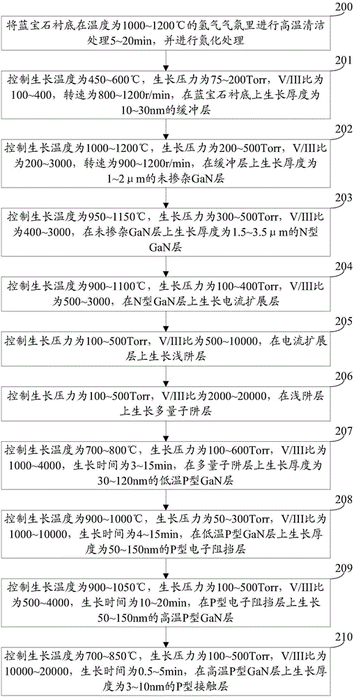
[0053] An embodiment of the present invention provides a method for growing an epitaxial wafer of a light emitting diode, which is suitable for growing the epitaxial wafer of a light emitting diode provided in Embodiment 1, see figure 2 , the growth method includes:
[0054] Step 200: Perform high-temperature cleaning treatment on the sapphire substrate in a hydrogen atmosphere at a temperature of 1000-1200° C. for 5-20 minutes, and perform nitriding treatment.
[0055] In this example, nitrogen (N 2) as carrier gas, trimethylgallium (TMGa), triethylgallium (TEGa), trimethylaluminum (TMAl), trimethylindium (TMIn) and ammonia (NH3) as Ga, Al, In And N source, use silane (SiH4) and dimagnesium (CP2Mg) as N and P type dopants respectively.
[0056] Step 201: Control the growth temperature to 450-600° C., the growth pressure to 75-200 Torr, the V / III ratio to 100-400, and the rotation speed to 800-1200 r / min, and grow a buffer layer with a thickness of 10-30 nm on the sapphire ...
Embodiment 3
[0085] An embodiment of the present invention provides a method for growing an epitaxial wafer of a light emitting diode. The difference between the growth method and the growth method provided in Embodiment 2 lies in that the thickness of each layer in the current spreading layer is different. Specifically, the thickness of the AlN layer is 2-3 nm, the thickness of the InGaN layer in the current spreading layer is 30-40 nm, and the thickness of the GaN layer in the current spreading layer is 12-16 nm.
PUM
| Property | Measurement | Unit |
|---|---|---|
| Thickness | aaaaa | aaaaa |
| Thickness | aaaaa | aaaaa |
| Thickness | aaaaa | aaaaa |
Abstract
Description
Claims
Application Information
 - R&D
- Intellectual Property
- Life Sciences
- Materials
- Tech Scout
- Unparalleled Data Quality
- Higher Quality Content
- 60% Fewer Hallucinations
Browse by: Latest US Patents, China's latest patents, Technical Efficacy Thesaurus, Application Domain, Technology Topic, Popular Technical Reports.
© 2025 PatSnap. All rights reserved.Legal|Privacy policy|Modern Slavery Act Transparency Statement|Sitemap|About US| Contact US: help@patsnap.com