Analog front-end circuit for fully-differential optical receiver based on adjustable common-emitter common-base structure
An analog front-end circuit and cascode technology, applied in the direction of electromagnetic receivers, can solve the problems of reducing gain, increasing chip area and noise, increasing design costs, etc., to achieve expanded bandwidth, improved single-stage gain, and good noise performance Effect
- Summary
- Abstract
- Description
- Claims
- Application Information
AI Technical Summary
Problems solved by technology
Method used
Image
Examples
Embodiment 1
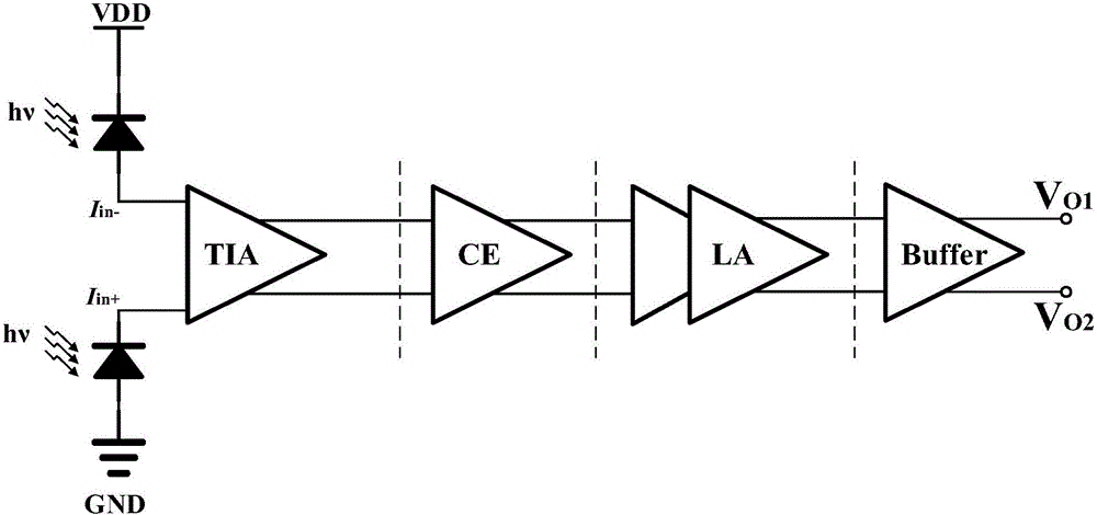
[0031] The embodiment of the present invention is based on the standard SiGe BiCMOS process, and proposes a fully differential optical receiver analog front-end circuit. The specific circuit includes:
[0032] Two photodetectors with completely symmetrical structures are used to convert the weak optical signal input by the optical fiber into a set of electrical pulse signals with opposite phases;
[0033] A transimpedance amplifier (TIA) with a one-stage differential structure is used to convert the weak current signal of the photodetector into a voltage signal and amplify it. The output terminal is connected with a first-stage emitter follower, which is used to increase the output load and reduce the DC level.
[0034] A common-emitter amplifier (CE) is used to improve the reverse isolation of the circuit and compensate the low-frequency pole of the circuit through capacitive degeneration technology. An emitter follower is cascaded at the output end to reduce the output DC l...
Embodiment 2
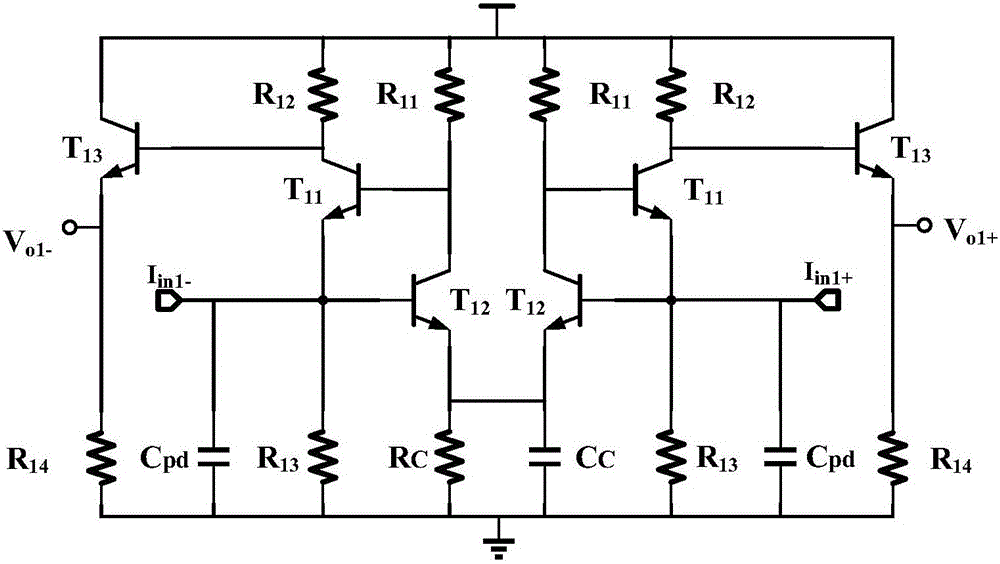
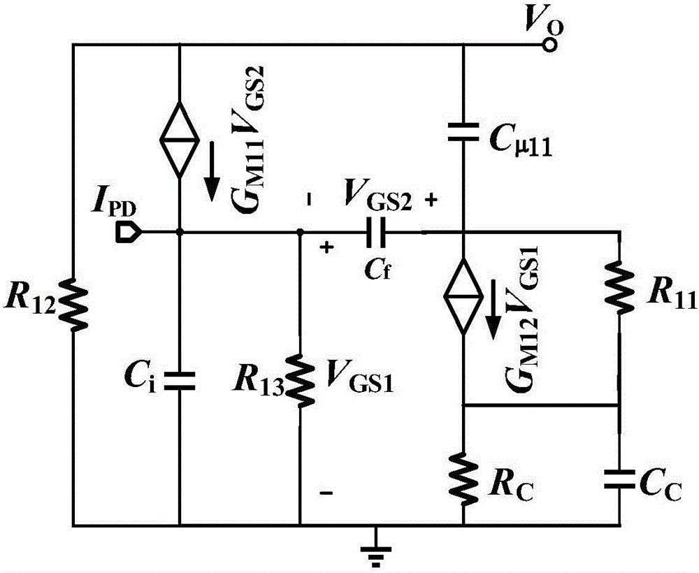
[0044] Combine below figure 2 , image 3 , Figure 4 , Figure 5 and Figure 6 The high-speed, high-gain optical receiver front-end analog circuit in Embodiment 1 is introduced in detail, see the following description for details:
[0045] figure 2 A preferred embodiment of differential structure regulated cascode (RGC) transimpedance amplifier is given. The circuit mainly includes: an RGC amplifier and an RC network that replaces the traditional tail current source, and its function is to amplify the weak signal current output by the photodetector and convert it into a voltage signal.
[0046] In addition to the RC network in the transimpedance amplifier (resistor R C with capacitance C C ), the circuit is completely symmetrical and identical. Detector Junction Capacitance C pd One end and input end, resistance R 13 , Transistor T 11The emitter and T 12 The base is connected, the other end is grounded; the resistor R 13 The other end of the ground; transistor T...
Embodiment 3
[0075] Combine below Figure 7 The feasibility verification of the high-speed, high-gain optical receiver analog front-end circuit in Embodiments 1 and 2 is described in detail below:
[0076] Figure 7 It is the amplitude-frequency curve response of the front-end analog circuit of a high-speed, high-gain optical receiver. The experimental process is well known to those skilled in the art, and will not be described in detail in this embodiment of the present invention.
[0077] The simulation results show that the total transimpedance gain of the circuit is 113dBΩ, and the -3dB bandwidth is 17.2GHz, which verifies the feasibility of the analog circuit and meets various needs in practical applications.
PUM
| Property | Measurement | Unit |
|---|---|---|
| Bandwidth | aaaaa | aaaaa |
Abstract
Description
Claims
Application Information


