

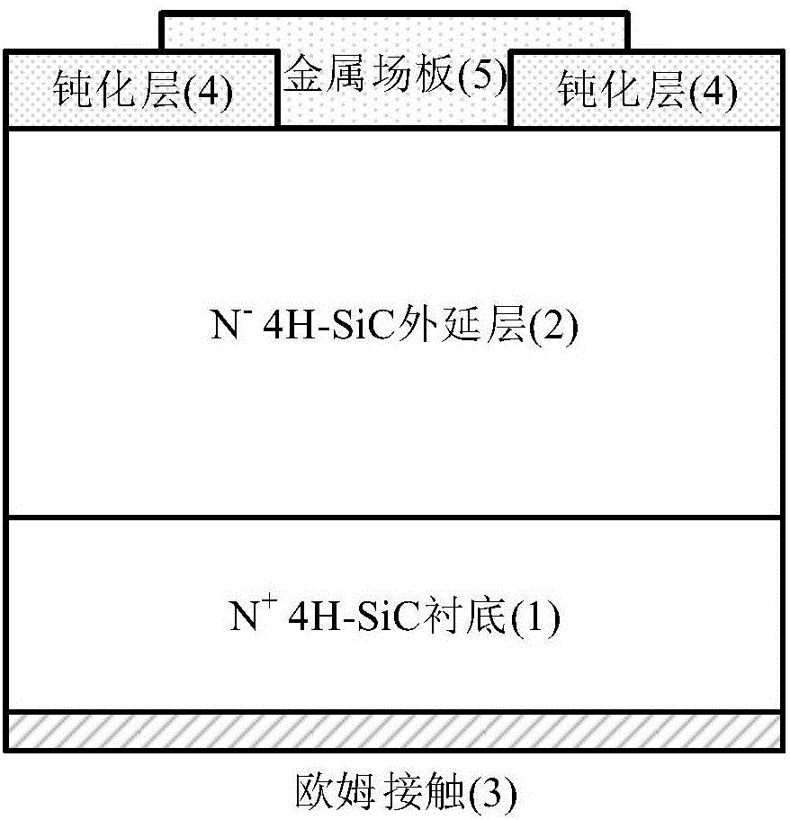
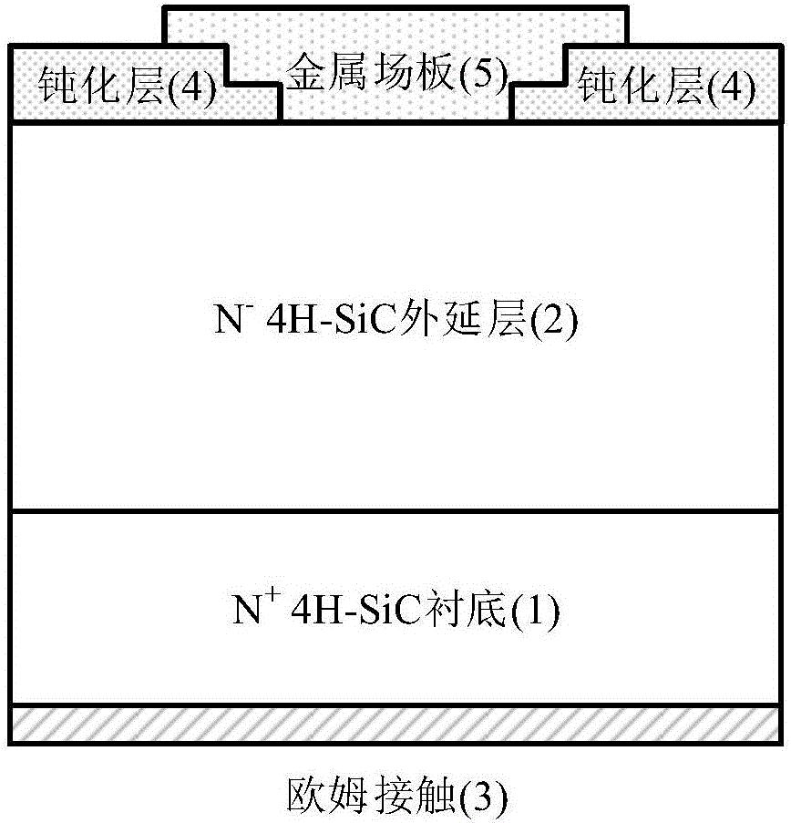
Double step field plate terminal based 4H-SiC Schottky diode and manufacturing method thereof
A technology of Schottky diodes and manufacturing methods, which is applied in semiconductor/solid-state device manufacturing, electrical components, electric solid-state devices, etc., can solve problems such as low breakdown voltage and uneven electric field distribution of passivation layer, and achieve improved breakdown voltage, avoiding premature breakdown, and increasing the length
- Summary
- Abstract
- Description
- Claims
- Application Information
AI Technical Summary
Problems solved by technology
Method used
Image

Examples
Embodiment 1
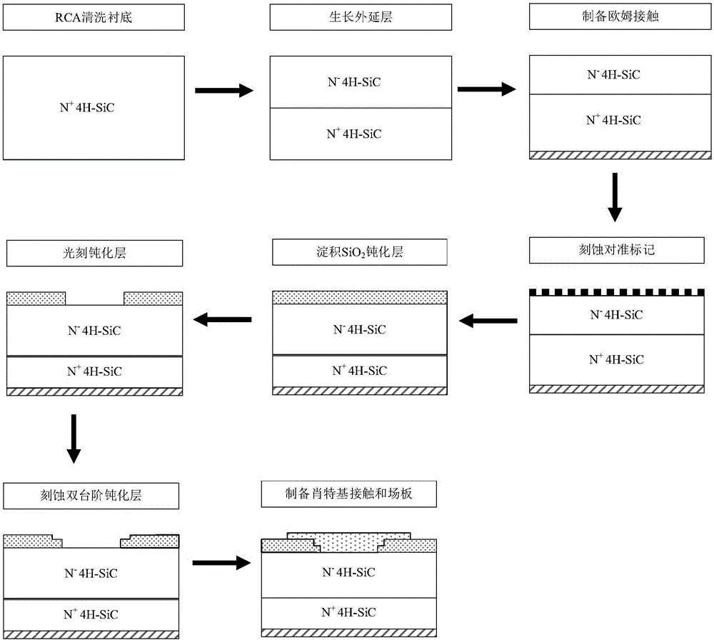
[0038] In Example 1, a 4H-SiC Schottky diode with a double-step field plate terminal with two steps with a thickness of 100 nm and 250 nm from top to bottom was fabricated.
[0039] Step 1. Select 4H-SiC substrate for standard RCA cleaning.
[0040] 1a) Choose a diameter of 2 inches and a doping concentration of 1×10 18 cm -3 Of N + 4H-SiC substrate;
[0041] 1b) Clean the selected SiC substrate with a mixed solution of 1:1:5 hydrochloric acid, hydrogen peroxide, and deionized water for 5 minutes to remove metal oxides, hydroxides and active metals on the substrate surface Impurities
[0042] 1c) Soak the cleaned substrate in a mixture solution of hydrogen fluoride and deionized water with a ratio of 1:10 for 30 seconds to remove natural oxides on the surface of the substrate;
[0043] 1d) Dry the cleaned substrate with nitrogen.
[0044] Step 2: Growing an epitaxial layer on the front surface of the substrate.
[0045] Use CVD method to grow the same type of N on the front surface of th...
Embodiment 2
[0085] Example 2: Fabrication of a 4H-SiC Schottky diode with a double-step field plate terminal with two steps with a thickness of 300 nm and 200 nm from top to bottom.
[0086] Step 1, select 4H-SiC substrate for standard RCA cleaning.
[0087] The specific implementation of this step is the same as step 1 of embodiment 1.
[0088] Step 2: Growing an epitaxial layer on the front surface of the substrate.
[0089] The specific implementation of this step is the same as step 2 of embodiment 1.
[0090] Step 3: Prepare ohmic contacts on the back of the substrate.
[0091] The specific implementation of this step is the same as step 3 of embodiment 1.
[0092] Step 4: etch the surface of the epitaxial layer to form alignment marks.
[0093] The specific implementation of this step is the same as step 4 of embodiment 1.
[0094] Step 5, deposit SiO on the surface of the epitaxial layer where the alignment mark is formed 2 Passivation layer.
[0095] 5.1) The PECVD method uses the following proc...
Embodiment 3
[0113] Embodiment 3: Fabrication of two stepped 4H-SiC Schottky diodes with a thickness of 300 nm from the top to the bottom of the double step field plate terminal.
[0114] Step A, select 4H-SiC substrate for standard RCA cleaning.
[0115] The specific implementation of this step is the same as step 1 of embodiment 1.
[0116] Step B, growing an epitaxial layer on the front surface of the substrate.
[0117] The specific implementation of this step is the same as step 2 of embodiment 1.
[0118] Step C, preparing an ohmic contact on the back of the substrate.
[0119] The specific implementation of this step is the same as step 3 of embodiment 1.
[0120] Step D, etching the surface of the epitaxial layer to form alignment marks.
[0121] The specific implementation of this step is the same as step 4 of embodiment 1.
[0122] Step E, depositing SiO on the surface of the epitaxial layer with alignment marks 2 Passivation layer.
[0123] First, set the PECVD process conditions as follows:
...
PUM
 Abstract
Description
Claims
Application Information