Avalanche photodiode with periodic nanostructure

An avalanche optoelectronic and nanostructure technology, which is applied in photovoltaic power generation, circuits, electrical components, etc., can solve the problems of reduced detection efficiency, sudden change of refractive index, and reduced reflection, so as to reduce the difficulty of implementation, simplify the preparation process, and improve industrial applicability Effect

Active Publication Date: 2016-10-26
UNIV OF SCI & TECH OF CHINA
View PDF5 Cites 7 Cited by
  • Summary
  • Abstract
  • Description
  • Claims
  • Application Information

AI Technical Summary

Problems solved by technology

The interface between silicon nitride and silicon will produce a sudden change in refractive inde

Method used


Image

  • Avalanche photodiode with periodic nanostructure
  • Avalanche photodiode with periodic nanostructure

Examples


Embodiment Construction

[0025] In order to make the object, technical solution and advantages of the present invention clearer, the present invention will be described in further detail below in conjunction with specific embodiments and with reference to the accompanying drawings.

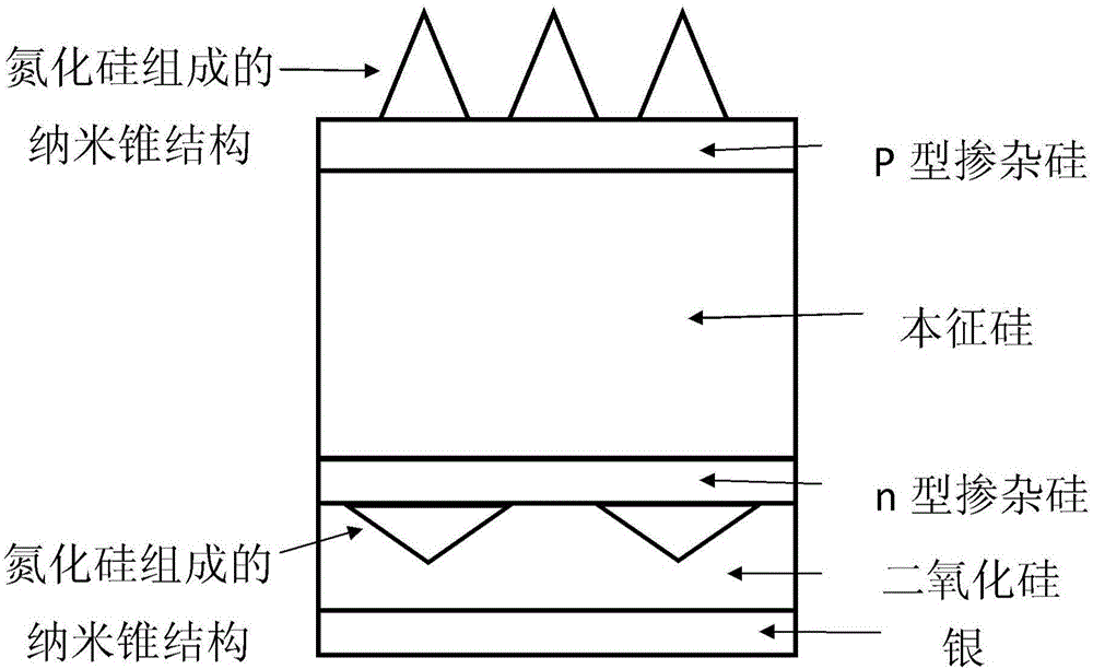
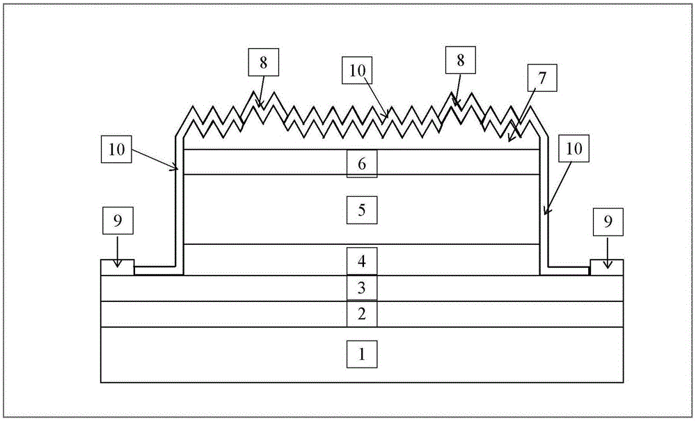
[0026] figure 2 A cross-sectional view of a single photon avalanche photodiode according to the present invention is shown. Such as figure 2 As shown, the single photon avalanche photodiode of the present invention is a circular mesa PIN structure, which includes Si substrate layer 1, SiO 2 SOI substrate composed of layer 2 and P+ ohmic contact layer 3.

[0027] On the SOI substrate, a P-transition layer 4, an intrinsic layer 5, an N-transition layer 6, and an N+ ohmic contact layer 7 are arranged in sequence, so that a circular mesa structure is formed on the SOI substrate. In addition, an annular N electrode layer 8 is formed on the N+ ohmic contact layer 7 near the outer periphery of the circular mesa, and an annu...


PUM

PropertyMeasurementUnit
Heightaaaaaaaaaa
Heightaaaaaaaaaa
Thicknessaaaaaaaaaa

Abstract

The invention provides a silicon-based avalanche photodiode applied to single photon detection in quantum information. The silicon-based avalanche photodiode comprises an SOI substrate and a PIN structure formed on the SOI substrate. A periodic Pyramid or inverted Pyramid shaped nanostructure is formed at the outermost layer of the PIN structure as an entrance window, wherein monocrystalline silicon is employed by the nanostructure as the main body material of a Pyramid basic unit. By using the avalanche photodiode structure of the invention, the preparation of the avalanche photodiode can be carried out by using an existing silicon-based preparation process, the layer structure of the diode is simplified, while the improved time resolution ability can be provided, good detection efficiency is provided, and the avalanche photodiode is suitable for industrialized production with a large scale and a high rate of finished products.

Description

technical field [0001] The invention relates to an avalanche photodiode, in particular to a silicon-based avalanche photodiode used in single photon detection in quantum information. Background technique [0002] In recent decades, the field of quantum information has received more and more attention, especially the rapid development of quantum secure communication in the past decade, which makes people feel that a new industry is about to mature. Because photons travel fast and are not easily affected by the environment, most quantum information technologies rely on photons for the preparation, regulation, transmission, and measurement of quantum states, thereby realizing the processing of quantum information. However, the energy of photons is very small, for example, for 850nm photons, its energy is only 2.3×10⁻¹⁹ joules. How to accurately and efficiently detect such weak energy photons is a key problem in quantum information. There are already many technical means to ach...

Claims


Application Information

Patent Timeline
IPC IPC(8): H01L31/107H01L31/0224H01L31/0232H01L31/0236
CPCY02E10/50H01L31/107H01L31/022408H01L31/02327H01L31/0236
Inventor 江晓张强臧凯马健丁迅霍秩杰喻宗夫詹姆斯S.哈里斯潘建伟
Owner UNIV OF SCI & TECH OF CHINA
Why Eureka
Try Eureka