Fabrication method for wafer-level mono-axial strain Si on AlN-buried insulation layer based on non-crystallization and scale effect

A uniaxial strain technology on an insulating layer, applied in the field of microelectronics, can solve the problems of non-adjustment, easy breakage, high cost, avoid damage and defects, improve insulation and heat dissipation, and improve material performance.

Active Publication Date: 2016-11-09
XIDIAN UNIV
View PDF6 Cites 45 Cited by
  • Summary
  • Abstract
  • Description
  • Claims
  • Application Information

AI Technical Summary

Problems solved by technology

The shortcoming of this invention is: only can make biaxially strained SOI material
Disadvantages of this invention: it is necessary to bend the Si wafer on the AlN buried insulating layer, which is easy to break, SiO 2 Buried insulating layer has poor heat dissipation, low flatness after springback of SOI sheet, and low yield
Disadvantages of this invention: only Si wafers on biaxially strained AlN buried insulating layer can be formed, there is a problem of Ge diffusion in the manufacturing process, and the amount of strain is small
[0013] Disadvantages of this invention: 1. SOI wafers with biaxial strain must be used, and the cost is higher
2. The strain in the top Si layer is fixed and cannot be adjusted in subsequent process steps
4. The nature of SOI strain is tensile strain, which can only increase the mobility of electrons, but not the mobility of holes.

Method used


Image

  • Fabrication method for wafer-level mono-axial strain Si on AlN-buried insulation layer based on non-crystallization and scale effect
  • Fabrication method for wafer-level mono-axial strain Si on AlN-buried insulation layer based on non-crystallization and scale effect
  • Fabrication method for wafer-level mono-axial strain Si on AlN-buried insulation layer based on non-crystallization and scale effect

Examples


Embodiment 1

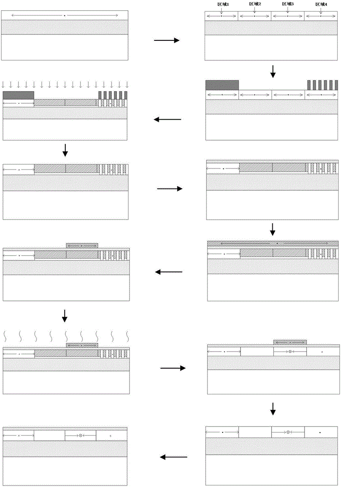
[0051] Example 1, making a wafer-level uniaxial tensile-strained Si material on a 5-inch AlN buried insulating layer.

[0052] Step 1: Select a 5-inch Si wafer on an AlN-buried insulating layer and clean it.

[0053] (1a) Use acetone and isopropanol to alternately perform ultrasonic cleaning on the Si wafer on the selected AlN buried insulating layer to remove organic contamination on the substrate surface;

[0054] (1b) Prepare a mixed solution of ammonia water, hydrogen peroxide, and deionized water in a ratio of 1:1:3, heat to 120°C, soak the Si wafer on the AlN-buried insulating layer in the mixed solution for 12 minutes, take it out and use Rinse with a large amount of deionized water to remove inorganic pollutants on the surface of the Si wafer on the AlN buried insulating layer;

[0055] (1c) Soak the Si wafer on the AlN buried insulating layer with HF acid buffer for 2 minutes to remove the oxide layer on the surface.

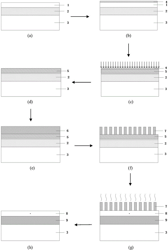
[0056] Step 2: Deposit SiO 2 Layer 4, such as ...

Embodiment 2

[0083] Example 2, manufacturing a wafer-level uniaxial tensile strained Si material on a 6-inch AlN buried insulating layer.

[0084] Step 1: Select a 6-inch Si wafer on an AlN-buried insulating layer and clean it.

[0085] The implementation of this step is the same as step 1 of Embodiment 1.

[0086] Step 2: Take out the Si wafer on the AlN buried insulating layer after cleaning, and deposit SiO on the top Si layer 1 by plasma-enhanced chemical vapor deposition PECVD process 2 layer, that is, the SiH 4 The flow rate is 45sccm, N 2 O flow is 164sccm, N 2 The flow rate is 800sccm, the gas pressure is 600mTorr, the power is 60W, and the deposition temperature is 300°C, and the SiO with a thickness of 16nm is deposited. 2 Layer 4, such as figure 2 (b) shown.

[0087] Step 3: Use an ion implanter to implant a dose of 3E15cm into the top Si layer 1 -2 , the energy is 60keV, Si ions to form an amorphous layer 5 inside the top Si layer 1, such as figure 2 (c) shown.

[0088...

Embodiment 3

[0098] Example 3, fabricating a wafer-level uniaxial compressively strained Si material on an 8-inch AlN buried insulating layer.

[0099] Step A: select an 8-inch Si wafer on an AlN buried insulating layer, and clean it.

[0100] The implementation of this step is the same as step 1 of Embodiment 1.

[0101] Step B: Deposit SiO 2 Layer 4, such as figure 2 (b) shown.

[0102] Take out the Si wafer on the AlN buried insulating layer after cleaning, and deposit SiO with a thickness of 25 nm on the top Si layer 1 by plasma enhanced chemical vapor deposition PECVD process. 2 Layer 4, prevents "channeling" from occurring, such as figure 2 (b) shown.

[0103] The deposition process is as follows: SiH 4 The flow rate is 45sccm, N 2 O flow is 164sccm, N 2 The flow rate is 800 sccm, the gas pressure is 600 mTorr, the power is 60 W, and the deposition temperature is 300° C.

[0104] Step C: forming an amorphized layer 5, such as figure 2 (c) shown.

[0105] Form SiO 2 Aft...


PUM

PropertyMeasurementUnit
thicknessaaaaaaaaaa
widthaaaaaaaaaa

Abstract

The invention discloses a fabrication method for wafer-level mono-axial strain Si on a AlN-buried insulation layer based on non-crystallization and a scale effect. The fabrication method is implemented according to the following steps of depositing a SiO2 layer at a Si layer at a top layer of a Si wafer on the cleaned AlN-buried insulation layer; performing ion injection on the Si layer at the top layer to form a non-crystallization layer, and removing the SiO2 layer on the non-crystallization layer; depositing a tensile stress SiN thin film or a press stress SiN thin film on the Si layer at the top layer, etching the SiN thin film to a mono-axial tensile stress SiN strip-shaped array or a mono-axial press stress SiN strip-shaped array, annealing the wafer to make the non-crystallization layer re-crystallized, and enabling the AlN-buried insulation layer to generate plastic deformation; and etching the SiN strip-shaped array to obtain the wafer-level mono-axial strain Si on the AlN-buried insulation layer. The wafer-level mono-axial strain Si has the advantages of high heat dissipation and large strain, and the fabrication method can be used for fabricating a wafer-level mono-axial strain Si material on the AlN-buried insulation layer.

Description

technical field [0001] The invention belongs to the field of microelectronics technology, and relates to semiconductor material manufacturing technology, in particular to a method for manufacturing wafer-level uniaxially strained Si on an AlN buried insulating layer, which can be used for manufacturing high temperature, high power consumption, high power semiconductor devices and integration High-performance SOI wafers required for circuits. Background technique [0002] With the development of Si-based semiconductor device manufacturing process, the continuous reduction of feature size is facing great challenges, that is, the continuous reduction of feature size will lead to the increase of parasitic capacitance, the deterioration of short channel effect, and the degradation of hot carriers. , Leakage is more serious, etc., resulting in a decline in device performance. [0003] SOI, or silicon on insulating layer, is a Si-based semiconductor substrate material with a three...

Claims


Application Information

Patent Timeline
Patent Type & Authority Applications(China)
IPC IPC(8): H01L21/762H01L21/02
CPCH01L21/0217H01L21/02274H01L21/7624
Inventor 戴显英焦帅郝跃吴武健苗东铭祁林林梁彬
Owner XIDIAN UNIV
Why Eureka
Try Eureka