Low-power fin type field effect transistor and manufacturing method thereof

A fin field effect, low-power technology, applied in semiconductor/solid-state device manufacturing, semiconductor devices, electrical components, etc., can solve problems such as large edge roughness, device characteristic consistency degradation, channel mobility degradation, etc. Achieve the effect of small leakage current, low cost and high on-state current

Active Publication Date: 2016-11-09
PEKING UNIV +1
View PDF4 Cites 1 Cited by
  • Summary
  • Abstract
  • Description
  • Claims
  • Application Information

AI Technical Summary

Problems solved by technology

However, if you want to form thinner and high-aspect-ratio Fin by etching, it poses a great challenge to the etching process, and the formation of ultra-thin Fin sidewalls by etching will have a large edge roughness , resulting in the degradation of the consistency of the device characteristics; in addition, in order to suppress the leakage of the deep body region, the doping of Fin will not only cause the degradation of the channel mobility, but also introduce a large random doping fluctuation (RDF), which limits The application of multi-gate devices in the field of low power consumption

Method used


Image

  • Low-power fin type field effect transistor and manufacturing method thereof
  • Low-power fin type field effect transistor and manufacturing method thereof
  • Low-power fin type field effect transistor and manufacturing method thereof

Examples


Embodiment Construction

[0080] The present invention will be described in detail below in conjunction with the accompanying drawings and specific examples.

[0081] A low-power N-type fin field-effect transistor with a fin-type isolation structure prepared on an SOI substrate can be realized according to the following steps:

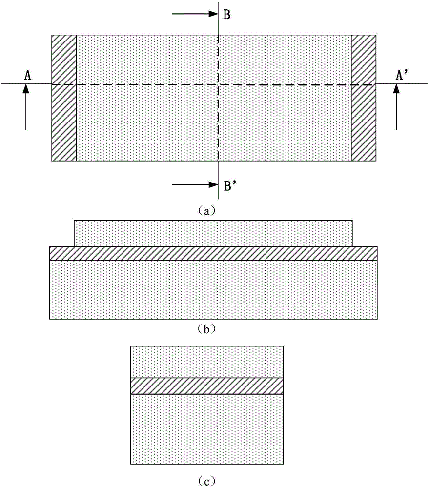
[0082] 1) On the P-type (100) SOI substrate, the HNA solution is used to thin the top silicon film to 250nm, and the active area of ​​the device is formed by photolithography and RIE etching, and the glue is removed, such as figure 1 shown;

[0083] 2) LPCVD SiO 2 300nm, the surface is planarized by chemical mechanical polishing to expose the upper surface of the active region and form STI, such as figure 2 shown;

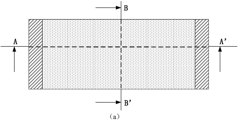
[0084] 3) LPCVD 200nm silicon oxide is used as the mask layer 1, and the pattern window of the fin-shaped spacer bar with a length of 100nm and a width of 30nm is defined by electron beam lithography, and the mask layer 1 and the mask layer 1 are anisotropical...


PUM


Abstract

The invention provides a low-power fin type field effect transistor and a manufacturing method thereof, and belongs to the technical field of super-large integrated circuit manufacture. The thickness of a sidewall channel layer and the thickness of a top channel layer of the field effect transistor are no greater than 10nm, and a fin-type isolation bar is formed on a deep body area far away from top gate control. Further shortening of a device trench length is facilitated, short channel effect control ability of the device is improved, and static power consumption is minimized. The source-drain area of the device is a monocrystalline active island, and has maller source-drain series resistance. Compared with a fin type field effect transistor employing lifting source-drain structure, the low-power fin type field effect transistor requires no epitaxial lifting source-drain to obtain rapidly high open-state current. The low-power fin type field effect transistor is compatible with conventional IC-manufacture technology and has the advantages of simple process and low manufacture cost.

Description

technical field [0001] The invention belongs to the technical field of ultra-large-scale integrated circuit manufacturing, and relates to a low-power consumption fin field effect transistor and a preparation method thereof. Background technique [0002] When semiconductor devices enter the 22nm technology generation, Fin Field Effect Transistor (FinFET) is a representative of three-dimensional multi-gate MOSFET (MuGFET), which has outstanding ability to suppress short channel effect and high integration density, and its preparation process Compatible with the traditional CMOS process, it has become the mainstream of semiconductor devices. However, when moving towards a smaller technology node, the deep body region of the three-dimensional multi-gate device is far away from the top gate control, which will cause a large leakage current and increase the static power consumption of the device. [0003] In order to overcome this problem, the method of thinning the Fin width is ...

Claims


Application Information

Patent Timeline
Patent Type & Authority Applications(China)
IPC IPC(8): H01L29/78H01L29/06H01L29/08H01L29/10H01L21/336
CPCH01L29/0642H01L29/0847H01L29/1033H01L29/66795H01L29/785
Inventor 黎明陈珙杨远程黄如
Owner PEKING UNIV
Why Eureka
Try Eureka