Transparent conductive laminated body and touch panel provided with transparent conductive laminated body

一种透明导电性、触摸面板的技术,应用在绝缘载体上的导电层、涂层、电子器材等方向,能够解决透明导电膜与接地电极短路、透明导电膜碎裂等问题,达到抑制离子迁移、可靠性优良、耐久性提高的效果

Inactive Publication Date: 2016-11-09
TOPPAN INC
View PDF5 Cites 6 Cited by
  • Summary
  • Abstract
  • Description
  • Claims
  • Application Information

AI Technical Summary

Problems solved by technology

[0009] In such a case, an electric field in a certain direction is generated between the ground electrode and the driving electrode or the sensing electrode. Therefore, depending on the material of the transparent conductive film used for the driving electrode or the sensing electrode, problems such as: Fragmentation of transparent conductive film caused by ion migration, or short circuit between transparent conductive film and ground electrode

Method used


Image

  • Transparent conductive laminated body and touch panel provided with transparent conductive laminated body
  • Transparent conductive laminated body and touch panel provided with transparent conductive laminated body
  • Transparent conductive laminated body and touch panel provided with transparent conductive laminated body

Examples


Embodiment 1

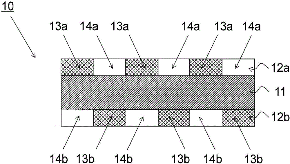
[0126] A UV curable resin was coated on one side of a PET substrate (75 μm), and a metal layer made of fibrous metal was formed thereon by a die coating method. Next, a solution containing an acrylic monomer as a main component was applied by a micro-gravure coating method so as to have a film thickness of 70 nm, and cured by UV irradiation to obtain a transparent conductive layer. A metal layer and a transparent conductive layer were also formed on the opposite side of the PET substrate by the same method. Next, a negative resist is applied by photolithography, after curing by UV irradiation, etching is performed with hydrochloric acid (0.1%), and the resist is stripped with sodium hydroxide solution (1%) to perform patterning. Forming and producing a plurality of strip-shaped conductive regions. In each of the strip-shaped conductive regions, a conductive paste based on epoxy resin and silver was used to form lead wires by screen printing, and a transparent conductive lamin...

Embodiment 2

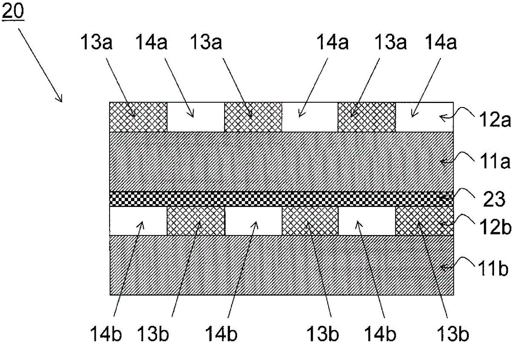
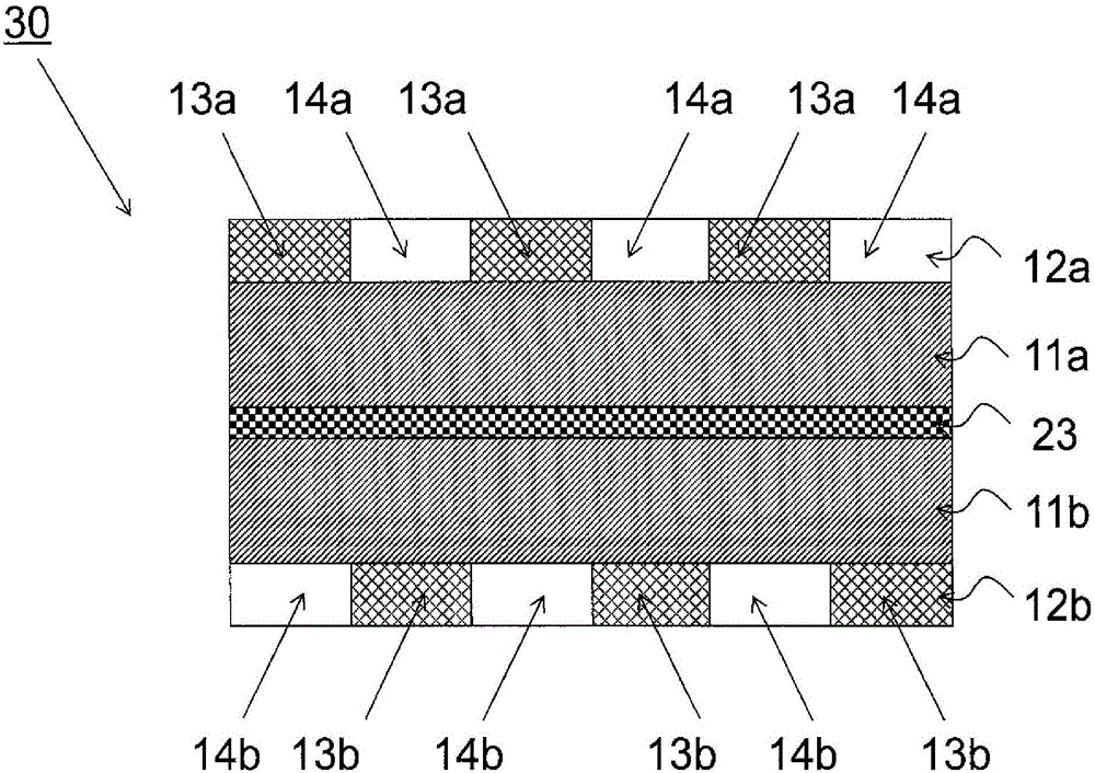
[0135] produced with Figure 18 The same layers constitute the touch panel 200 . Figure 19 is a plan view showing the electrode portion of the touch panel 200, and a schematic cross-sectional view taken along the B line is Figure 18 . Using PET (125 μm) as the substrate 11, UV curable transparent acrylic resin added with 20 wt% of UV absorber was microgravure coated on both sides, dried and UV cured, thereby forming the resin layer 2 as A thickness of 5 μm is formed on both surfaces of the substrate 11 . On both sides of the obtained base material, as the material of the transparent electrode layers 12a, 12b, the transparent electrode layers 12a, 12b were formed by coating silver nanowires by slot die coating so that the square resistance became 100Ω / □. 12b, similarly, a UV curable transparent acrylic resin was applied to a thickness of 130 nm to form a cured film.

[0136] For the substrate on which the transparent electrode layers 12a, 12b are formed on both sides, aft...


PUM

PropertyMeasurementUnit
contact resistanceaaaaaaaaaa
heat shrinkage ratioaaaaaaaaaa
coating thicknessaaaaaaaaaa

Abstract

Provided are: a transparent conductive laminated body wherein malfunction does not occur at high temperatures and high humidity; and a touch panel that is provided with the transparent conductive laminated body. The transparent conductive laminated body is provided with: a transparent base material; and a transparent electrode layer, which is laminated on one surface or both surfaces of the transparent base material, and which contains a resin. The transparent electrode layer includes a plurality of conductive regions having a fibrous metal, and a plurality of nonconductive regions, and the thickness of the transparent electrode layer is 30-150 nm.

Description

technical field [0001] The technology of the present invention relates to a transparent conductive laminate and a touch panel including the transparent conductive laminate. Background technique [0002] In recent years, capacitive touch panels have been widely used as input devices of electronic equipment. The projected capacitive touch panel has two electrodes for detecting changes in capacitive capacitance. The two electrodes face each other via a transparent substrate. These electrodes are formed by patterning a transparent conductive film formed on a substrate. [0003] Indium tin oxide (ITO) is typically used as a material for a transparent conductive film formed on a substrate as an electrode. The method of forming an ITO film on a substrate is dry vacuum film formation. However, since indium, which is a main component of ITO, is a rare metal, there is concern about its stable supply, and there is also a problem of lack of flexibility. In addition, the manufacturi...

Claims


Application Information

Patent Timeline
Patent Type & Authority Applications(China)
IPC IPC(8): G06F3/044B32B7/02G06F3/041H01B5/14
CPCB32B3/10B32B5/02B32B5/028B32B5/142B32B7/12B32B15/02B32B15/08B32B15/082B32B15/20B32B27/06B32B27/08B32B27/12B32B27/36B32B2255/02B32B2255/06B32B2255/26B32B2260/021B32B2262/103B32B2307/202B32B2307/206B32B2307/412B32B2457/208G06F3/0445Y10S977/762B32B2309/105G06F3/044G06F2203/04111G06F3/041
Inventor 岩田玲子伊藤大
Owner TOPPAN INC
Why Eureka
Try Eureka