
P-type amorphous oxide semiconductor including gallium, method of manufacturing same, and solar cell including same and method of manufacturing said solar cell

Preparing gallium-containing p-type oxide semiconductors through a solution process solves the problem of developing high-performance materials at low temperatures and the problem of low charge mobility in organic solar cells, achieving low-cost and efficient solar cell manufacturing.

Active Publication Date: 2016-11-09
UNIVERSITY INDUSTRY COOPERATION GROUP OF KYUNG HEE UNIVERSITY
View PDF6 Cites 1 Cited by
  • Summary
  • Abstract
  • Description
  • Claims
  • Application Information

AI Technical Summary

Problems solved by technology

[0027] As mentioned above, the advantages of oxide semiconductors are high mobility and high band gap, but they are mainly published as n-type due to oxygen vacancies (oxygen-vacancies) and zinc interstitials (zinc interstitials), and the disadvantage is that it is difficult to p-type doping ( doping)

Method used


Image

  • P-type amorphous oxide semiconductor including gallium, method of manufacturing same, and solar cell including same and method of manufacturing said solar cell
  • P-type amorphous oxide semiconductor including gallium, method of manufacturing same, and solar cell including same and method of manufacturing said solar cell
  • P-type amorphous oxide semiconductor including gallium, method of manufacturing same, and solar cell including same and method of manufacturing said solar cell

Examples


Embodiment

[0106] Prepare precursor solution

[0107] CuCl 2 , NH 2 CSNH 2 (Thiourea), Ga(NO 3 ) 3 ·xH 2 O(Galliumnitrate hydrate), SnCl 2 The precursor solution was prepared by dissolving into acetonitrile and ethylene glycol solvents.

[0108] active layer

[0109] After spin-coating the prepared precursor solution, heat treatment on a hot plate at 240° C. for about 1 minute, or perform inkjet printing on a substrate at 60° C. to form an active layer.

[0110] heat treatment step

[0111] The active layer formed by the spin coating or inkjet printing is annealed in a nitrogen atmosphere at a temperature of 300° C. for about 1 hour.

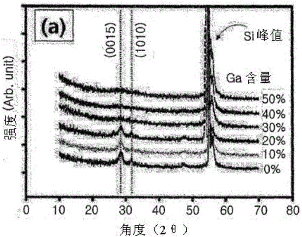
[0112] Semiconductor oxide analysis

[0113] figure 1 Show CuS-Ga x sn 1-x XRD results when the Ga concentration in the O film is 0-50%.

[0114] CuS-Ga x sn 1-x O has a polycrystalline structure (2θ=28°, 32°), and changes from a crystalline state to an amorphous state when the concentration of Ga is 30% or more.
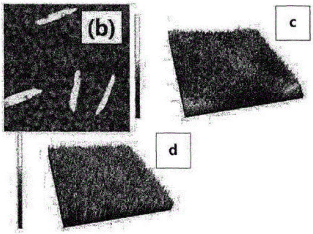
[0115] figure ...


PUM


Abstract

The present invention discloses a p-type amorphous oxide semiconductor including gallium, a method of manufacturing same, and a solar cell including same and a method of manufacturing the solar cell. According to the present invention, a p-type oxide semiconductor is provided in which Ga is additionally combined with a compound of CuS and one or more selected from SnO, ITO, IZTO, IGZO, and IZO.

Description

technical field [0001] The present invention relates to a P-type amorphous oxide semiconductor containing gallium, a method for manufacturing the same, a solar cell containing the same, and a method for manufacturing the same. Background technique [0002] Oxide semiconductors have recently attracted attention as materials for electronic books (e-books) that can replace various publications such as newspapers, journals, textbooks, and books, and as materials for flexible displays that can be bent, and research on this is very active. [0003] This is because oxide semiconductors have high mobility and are transparent, so transparent displays can be easily obtained, and they are also evaluated as alternative technologies capable of overcoming the critical point of conventional technologies. [0004] That is, in terms of current silicon (Si)-based technology, a-Si-based thin-film transistor (TFT) elements, which are switching elements used to activate OLEDs that are attracting...

Claims


Application Information

Patent Timeline
Patent Type & Authority Applications(China)
IPC IPC(8): H01L51/42H10K99/00
CPCY02E10/549Y02P70/50H10K85/1135H10K85/215H10K85/113H10K30/152H10K30/50H10F77/12H01L2224/05105H01L2924/10471H01L2924/10724H01L2224/05147H01L2224/05247H01L2924/10524H01L2224/05211H10K30/15H10F10/16H10F71/00H10D30/6756
Inventor 张震克里斯托夫·文森特·艾维金炯弼
Owner UNIVERSITY INDUSTRY COOPERATION GROUP OF KYUNG HEE UNIVERSITY
Learn More