
NO2 sensor and preparation method thereof
A technology of sensors and epitaxial thin films, which is applied in the field of NO2 sensors based on WO3 epitaxial thin films and its preparation, can solve the problems of reduced sensitivity, low barriers to mass production repeatability, long response time, etc., to achieve improved detection capabilities and stability, micro Compatibility with processing technology and the effect of improving detection efficiency
- Summary
- Abstract
- Description
- Claims
- Application Information
AI Technical Summary
Problems solved by technology
Method used
Image

Examples
Embodiment 1
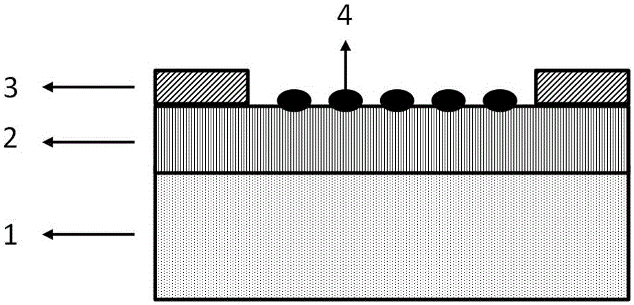
[0027] See attached figure 1 , which is the NO provided by this example 2 Schematic diagram of the sensor structure with SrTiO 3 (001) is a single crystal substrate, and the sensor adopts the laser molecular beam epitaxy (Laser-MBE) method to grow WO on the oxide single crystal substrate 1 3 Epitaxial film 2, and then prepare test electrode 3, and in WO 3 Precious metal catalyst particles 4 are deposited on the surface of the epitaxial film to produce NO 2 sensor. The specific production process is as follows:
[0028] (1) Cleaning SrTiO 3 (001) single crystal substrate. SrTiO 3 (001) The single crystal substrate was ultrasonically cleaned in acetone solution for 5 minutes, rinsed with deionized water and corroded in HF solution for 5 minutes, then rinsed with deionized water and dried to obtain a clean single crystal substrate.
[0029] (2) Growing WO 3 epitaxial film. SrTiO 3 The (001) single crystal substrate is placed in a laser molecular beam epitaxy device an...
Embodiment 2
[0036] The materials and process steps used in this example are basically the same as in Example 1, only the WO in step (2) 3 The growth rate of the epitaxial film was adjusted to 10 nm / s.
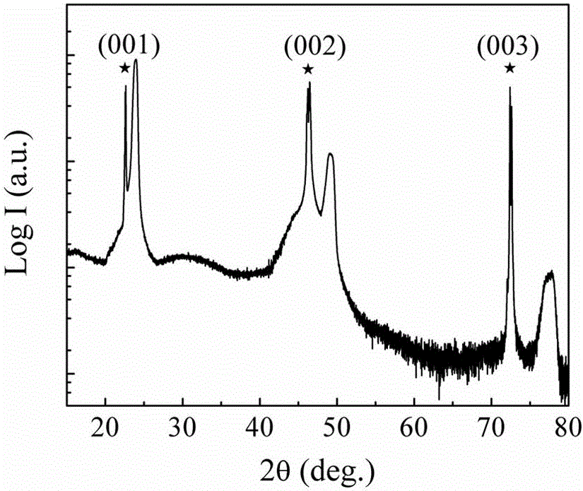
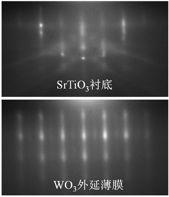
[0037] XRD and RHEED test results show that the deposited WO 3 The film is an epitaxial film with good crystalline quality, and its effect on NO 2 The test result is comparable with embodiment 1.
Embodiment 3
[0039] NO provided by this example 2 Sensor, the preparation steps are as follows:
[0040] (1) Cleaning SrTiO 3 (001) single crystal substrate. SrTiO 3 (001) The single crystal substrate was ultrasonically cleaned in acetone solution for 5 minutes, rinsed with deionized water and corroded in HF solution for 5 minutes, then rinsed with deionized water and dried to obtain a clean single crystal substrate.
[0041] (2) Growing WO 3 epitaxial film. SrTiO 3 The (001) single crystal substrate is placed in a laser molecular beam epitaxy device and heated to 600°C. Bombardment of WO with 1Hz, 350mW pulsed KrF laser 3 solid target surface, enabling WO 3 Material evaporates instantly and deposits onto SrTiO 3 (001) single crystal substrate surface to obtain WO 3 For epitaxial thin films, the growth rate is about 0.01nm / s.
[0042] (3) Sputtering deposition method in WO 3 Fabrication of Pt particles on the surface of epitaxial thin film as NO 2 detected catalyst.
[0043]...
PUM
 Abstract
Description
Claims
Application Information