Removal method of LED electrode structure

A technology of electrode structure and metal electrode, which is applied in the direction of circuits, electrical components, semiconductor devices, etc., can solve problems such as inapplicable rework treatment, and achieve the effects of complete and effective corrosion rework, wide application range, and simple operation

Active Publication Date: 2016-11-16
SHANDONG INSPUR HUAGUANG OPTOELECTRONICS
View PDF7 Cites 12 Cited by
  • Summary
  • Abstract
  • Description
  • Claims
  • Application Information

AI Technical Summary

Problems solved by technology

The method mentioned in this patent has high selectivity and can retain the original ITO layer. This method can be used for LED wafers that confirm the integrity of the ITO layer. At the same time, this advantage also limits that this method cannot be applied to all electrodes. Rework

Method used


Image

  • Removal method of LED electrode structure
  • Removal method of LED electrode structure
  • Removal method of LED electrode structure

Examples


Embodiment

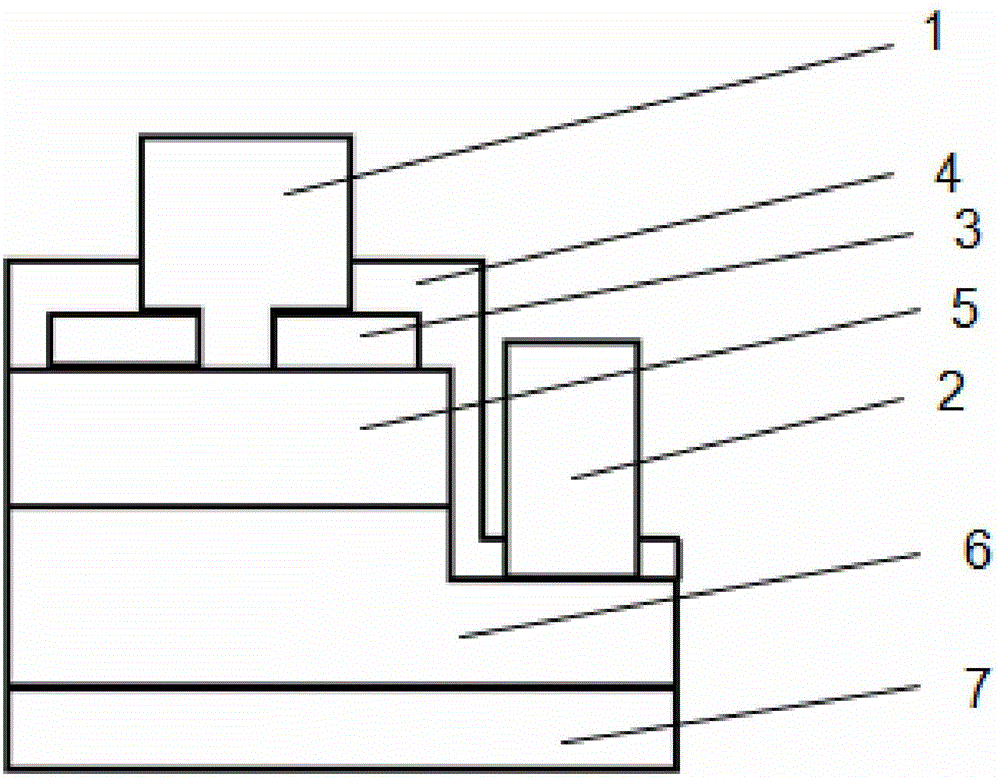
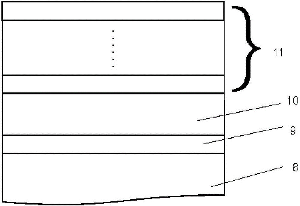
[0043]A method for removing a sapphire wafer LED tube core, the sapphire wafer LED tube core comprising a sapphire substrate layer 7, N-type gallium nitride, 6, a P-type gallium nitride layer 5, an ITO layer 3, and a silicon dioxide protection layer 4 , P electrode 1, N electrode 2, P electrode 1, N electrode 2 are made of metal electrode layer, the metal electrode layer is provided with sapphire substrate 8, metal chromium layer 9, metal aluminum layer 10, mixed metal layer in sequence from bottom to top Layer 11, mixed metal layer 11 is provided with metal platinum layer, metal gold layer successively from bottom to top, and the thickness of silicon dioxide protection layer 4 is The thickness of the ITO layer 5 is The thickness of metal chromium layer 9 is The thickness of the metal aluminum layer 10 is The thickness of the platinum layer is The thickness of the metal gold layer is Schematic diagram of the structure of the sapphire wafer LED die figure 1 As shown,...


PUM

PropertyMeasurementUnit
Densityaaaaaaaaaa
Densityaaaaaaaaaa
Densityaaaaaaaaaa

Abstract

The invention relates to a removal method of an LED electrode structure. The removal method comprises the following steps of firstly, initially reducing adhesion between a metal electrode layer and a P-GaN layer through physical ultrasound; secondly, corroding a surface protection layer with hydrofluoric acid; and finally, removing all metal (comprising titanium, gold beryllium, gold, platinum, silver, nickel and germanium) in which metal chromium and aluminum are taken as a bottom layer in the metal electrode layer by a mixed solution of hydrochloric acid and hydrogen peroxide. According to the removal method, a relatively thin strip of chromium at the bottommost layer is removed in a specific environment and metal arranged at an aluminum top layer can also drop off with aluminum mainly through reaction of metal aluminum and dilute acid. The removal method has the advantages of simple steps and simplicity in operation, the whole metal electrode layer is completely and effectively corroded and remade on the condition that a special chromium corrosion liquid, a gold corrosion liquid and the like is not used and on the premise that no damage is completely ensured, the LED electrode structure after being corroded and cleaned is clean in surface, and no any metal residue and bottom membrane residue at a chromium layer are generated.

Description

technical field [0001] The invention relates to a method for removing an LED electrode structure, in particular to a method for removing a sapphire substrate with a silicon dioxide protective layer and a gallium nitride-based LED electrode structure with a chrome-aluminum metal as the bottom layer, belonging to the technical field of semiconductor processing . Background technique [0002] LED (Light Emitting Diode) is made of several layers of very thin doped semiconductor materials, one of which has excess electrons, while the other layer forms positively charged "holes" because there are no electrons. When there is current As they pass through, electrons and holes combine with each other and release energy, which radiates light. Moreover, LED is an energy-saving and environment-friendly light source, which has the advantages of high luminous efficiency, long service life, strong safety and reliability, and low power consumption. It is precisely because of these advantage...

Claims


Application Information

Patent Timeline
IPC IPC(8): H01L33/00
Inventor 徐晓强彭璐闫宝华刘琦
Owner SHANDONG INSPUR HUAGUANG OPTOELECTRONICS
Why Eureka
Try Eureka