


Quick Research
Generate reliable direction feasibility study reports for your R&D in just a few steps.

Technical Q&A
Discover and master advanced knowledge NOW. Basics, ideas, possibilities, all at once.

Find Solutions
As an expert in R&D theories, this can generate solutions to your technical problems instantly.

Evaluate Feasibility
Analyze your overall solution with one click, know your potential R&D risks in advance.

Monitor Landscape
Get weekly tech updates, stay abreast of the latest tech innovations and key insights.
Calibration method for heat processing unit
A correction method, correction value technology, applied in the field of microelectronics and microtechnology, which can solve the problems of approximation, failure to take into account the heating zone, the impact of the output of the operation, etc.
- Summary
- Abstract
- Description
- Claims
- Application Information
AI Technical Summary
Problems solved by technology
Method used
Image

Examples
example 1
[0090] Common processing treatments applied to SOI substrates include smoothing annealing, which involves exposing the upper layer of silicon to a neutral or reducing atmosphere at elevated temperatures (typically above 1100°C). The treatment makes it possible, among other things, to reduce the roughness of layers exposed to high temperature atmospheres by surface reconstruction.
[0091]The treatment also changes the properties of the underlying dielectric layer, such as its thickness, by virtue of the oxide decomposition effect. This phenomenon is specifically reported in the document "Novel trends in SOI Technology for CMOS applications" by O. Kononchuck et al. This document actually explains that under a high temperature neutral or reducing processing atmosphere, the oxygen atoms of the dielectric layer tend to diffuse through the upper layer and react with its surface, producing volatile particles that are evacuated through the furnace atmosphere.
[0092] An important p...
example 2
[0103] Another common type of thermal treatment in the silicon and SOI field is thermal oxidation. For the manufacture of SOI substrates, especially by the Smart Cut process, a thermal oxide layer is typically grown on at least one of the substrates to be assembled. This oxide layer will constitute the buried oxide layer of the final SOI structure.
[0104] The oxide thickness is measured at multiple points (eg, 40 points) of the processed substrate. From these measurements an average is derived which corresponds to the properties of the substrate monitored for the process. It generally has to be between the control limits defined for the process according to the + / -3sigma rule.
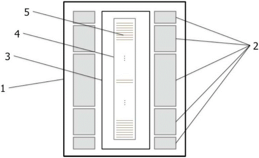
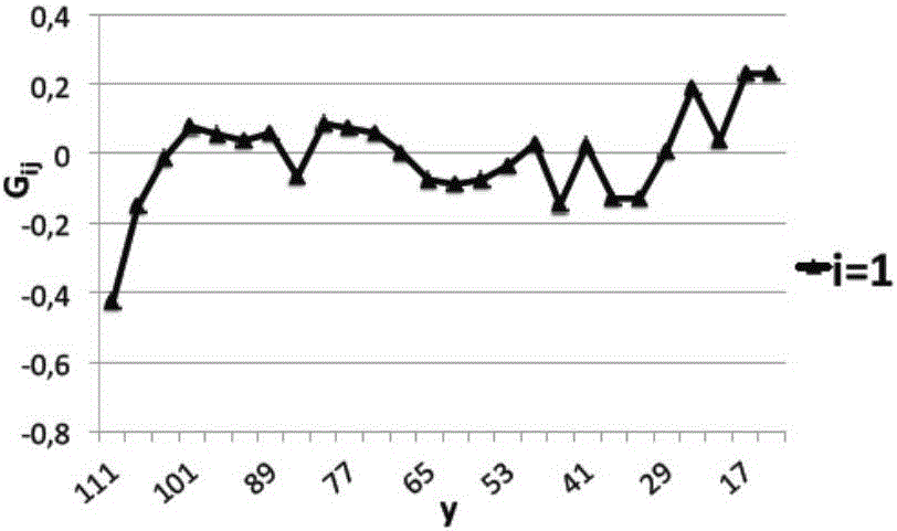
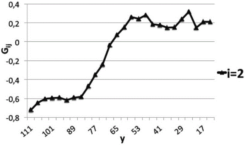
[0105] In the type of thermal processing unit considered for this process, the number of substrate positions is 150 and the number of heating zones is 5.
[0106] The sensitivity model was generated based on 25 measurement locations regularly distributed along the reactors of the entire furnace an...
example 3
[0113] The correction method can also be applied to single wafer thermal processing units, such as RTA (rapid thermal annealing) or RTP (rapid thermal processing) units, which enable, for example, a surface smoothing process at very high temperatures in a very short time. In this case, the reactor is not a large-sized tube, but a chamber capable of accommodating a single wafer. The uniformity of heating does not become trivial because the processes performed in these units are performed at very high temperatures, with very fast temperature rises: if the temperature at the substrate is not controlled, the same The fast reaction kinetics can create a large amount of inhomogeneity. The heating element consists of a halogen lamp.
[0114] The verified substrate properties are the substrate roughness measured by DRM (Differential Reflectance Microscopy), a technique based on the correlation of the optical reflectivity of a layer with its thickness, as explained in document WO2014 / ...
PUM
 Abstract
Description
Claims
Application Information
 - R&D Engineer
- R&D Manager
- IP Professional
- Industry Leading Data Capabilities
- Powerful AI technology
- Patent DNA Extraction
Browse by: Latest US Patents, China's latest patents, Technical Efficacy Thesaurus, Application Domain, Technology Topic, Popular Technical Reports.
© 2024 PatSnap. All rights reserved.Legal|Privacy policy|Modern Slavery Act Transparency Statement|Sitemap|About US| Contact US: help@patsnap.com