Micro-bolometer based on graphene quantum points

A technology of graphene quantum dots and microbolometers, which is applied in the direction of electric radiation detectors, electrical components, circuits, etc., can solve the problems of small temperature coefficient of resistance, difficulty in the middle and far infrared bands, and work restrictions, and achieve increased Effect of temperature change, high substrate compatibility, strong compatibility

Active Publication Date: 2016-12-07
CHONGQING INST OF GREEN & INTELLIGENT TECH CHINESE ACADEMY OF SCI
View PDF8 Cites 10 Cited by
  • Summary
  • Abstract
  • Description
  • Claims
  • Application Information

AI Technical Summary

Problems solved by technology

In terms of photon type, graphene-based photodetectors can already achieve a responsivity exceeding 1.0E+9A / W, but they are mainly concentrated in the visible light band, and it is difficult to be used in the mid-to-far infrared band
In terms of photothermal type, the thin layer characteristics of graphene and relatively weak phonon-electron interaction make the photogenerated carrier temperature of graphene material change greatly, but it is precisely because of the weak phonon-electron interaction , so the temperature coefficient of resistance is small, and special measures need to be taken to increase the temperature coefficient of resistance
According to the report in the literature (see J.Yan, M-H.Kim, et al., "Dual-gated bilayergraphene hot-electron bolometer", Nature Nanotechnology, 7,472, 2012), by using double-layer graphene as a photoresponse unit for radiometry Thermometers, temperature coefficients of resistance as high as 22kΩ / K have been achieved, however operating work is limited to less than 10K
In terms of patents, the current photodetectors based on graphene materials are mainly photon-based, such as the Chinese patent "A photodetector based on twisted double-layer graphene and its preparation method" CN201510078677 filed by Liu Zhongfan and others in 2015 .1, while photothermal-based, especially graphene-based microbolometers have relatively little patent protection

Method used


Image

  • Micro-bolometer based on graphene quantum points
  • Micro-bolometer based on graphene quantum points

Examples


specific Embodiment

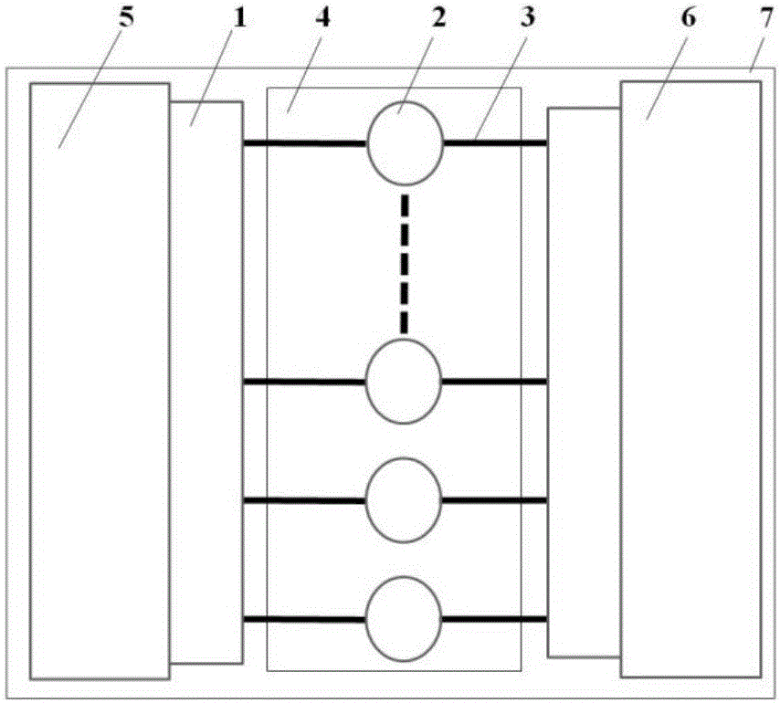
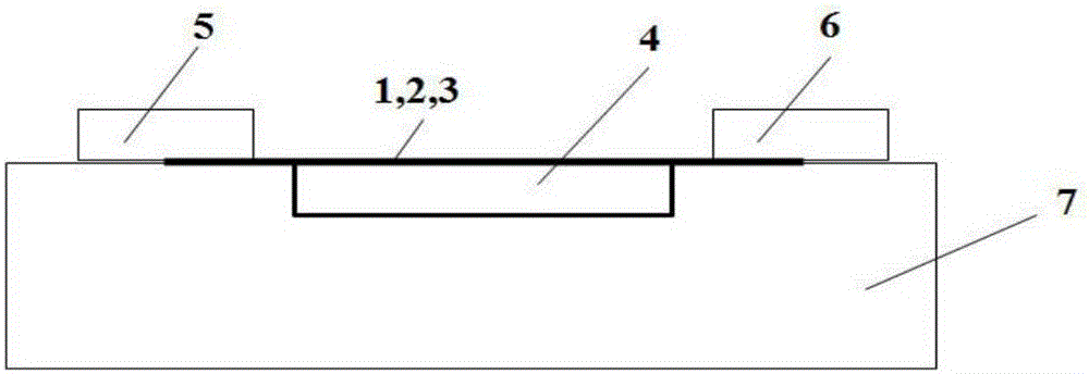
[0036] The concrete device that the present invention proposes in detail below in conjunction with accompanying drawing, as figure 1 and figure 2 shown. The structure of the graphene quantum dot microbolometer includes: graphene electrodes 1, graphene quantum dots 2, graphene strips 3, grooves 4, metal electrodes 5, 6 and a substrate 7. Specific examples are as follows:

[0037] This embodiment adopts the following specific schemes:

[0038] 1), substrate 7 preparation: the substrate 7 of the present invention is generally an insulating substrate or a conductive substrate covered with an insulating layer, without other requirements. In this embodiment, a substrate covered with 100 nm to 500 nm silicon oxide is used A heavily doped silicon wafer is used as the substrate 7 .

[0039]2), Groove 4 etching: use photolithography + wet etching process, use diluted HF acid (HF saturated solution: H 2 O=10:1) Etch away part of the silicon oxide on the surface of the silicon wafer...


PUM

PropertyMeasurementUnit
diameteraaaaaaaaaa
widthaaaaaaaaaa
lengthaaaaaaaaaa

Abstract

The invention provides a micro-bolometer based on graphene quantum points. The micro-bolometer comprises a substrate whose middle part is provided with a groove. The graphene quantum points are hanged above the groove and are connected through a graphene strip. Two ends of the graphene strip extend out of a graphene film to cover the substrate at two sides of the groove to form graphene electrodes. The micro-bolometer is characterized in that a hanged island-shaped graphene quantum point array is formed through the micro nano processing technology, the device temperature change in a same incident light power is increased by using the heat insulation effect by groove suspension, the device resistance temperature coefficient is raised by using quantization graphene, and the photoelectric detection is realized based on a micro-bolometer principle. Due to the absorption characteristic of a graphene material in an infrared wave band, the micro-bolometer provided by the invention can be used for the photoelectric detection of middle and far-infrared and terahertz wave bands, and a novel solution is provided for a present infrared photoelectric detector.

Description

technical field [0001] The invention belongs to the technical field of mid-far infrared and terahertz photoelectric detection, and relates to a graphene quantum dot-based microbolometer for photoelectric detection. Background technique [0002] Infrared detector is a photosensitive device that can convert infrared radiation energy into electrical energy. Due to its good environmental adaptability, good concealment, and strong anti-interference ability, it is widely used in military, meteorological, industrial, agricultural and forestry, Environmental science, public security security and medical diagnosis and other fields. [0003] In the mid-to-far infrared and terahertz bands, due to the limitation of photon energy, photon-type photodetectors generally require redundant refrigeration equipment (participate in A.Rogalski, "Infrared Detectors for the Future", ACTA PHYSICAPOLONICA A, 3,389, 2009), so currently The photodetectors in the middle and far infrared bands are mainl...

Claims


Application Information

Patent Timeline
Patent Type & Authority Applications(China)
IPC IPC(8): G01J5/20H01L31/09
CPCG01J5/20H01L31/09
Inventor 申钧魏兴战冯双龙魏大鹏杨俊周大华史浩飞杜春雷
Owner CHONGQING INST OF GREEN & INTELLIGENT TECH CHINESE ACADEMY OF SCI
Why Eureka
Try Eureka