Semiconductor device and semiconductor module

A technology for semiconductors and mounting substrates, used in semiconductor devices, semiconductor/solid-state device manufacturing, semiconductor/solid-state device components, etc., can solve problems such as MOSFET malfunctions, reduce failure rates, improve heat dissipation efficiency, and prevent malfunctions. Effect

Inactive Publication Date: 2016-12-14
PANASONIC INTELLECTUAL PROPERTY MANAGEMENT CO LTD
View PDF7 Cites 7 Cited by
  • Summary
  • Abstract
  • Description
  • Claims
  • Application Information

AI Technical Summary

Problems solved by technology

Therefore, if the resistor and the MOSFET are placed close to each other, the MOSFET may malfunction due to the heat generated from the resistor.

Method used


Image

  • Semiconductor device and semiconductor module
  • Semiconductor device and semiconductor module
  • Semiconductor device and semiconductor module

Examples


Embodiment approach 1

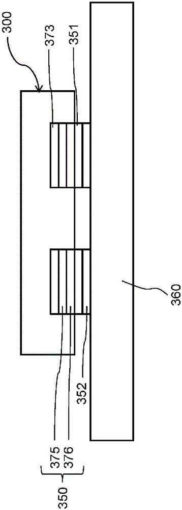
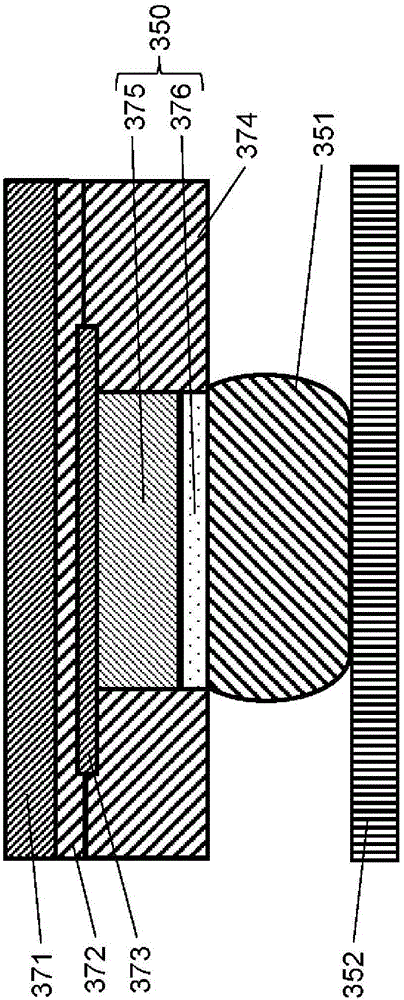
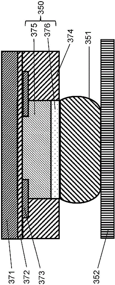
[0060] Below, use Figure 1 ~ Figure 3 The connection between the MOSFET type semiconductor device and the printed wiring board (mounting board) of the semiconductor module on which the MOSFET type semiconductor device according to the first embodiment is mounted will be described. A semiconductor module is a product form in which a MOSFET type semiconductor device is mounted on a printed wiring board and integrated. figure 1 This is an example in which a semiconductor device in a BGA (Ball grid array) type chip size package is surface-mounted on a printed wiring board. Such as figure 1 As shown, the semiconductor device 300 is turned upside down so that the printed wiring board 360 on which the cell balancing circuit is mounted faces the surface of the semiconductor device 300 on which the surface mount terminals 350 are mounted. Then, the copper wiring (terminal bonding portion) 352 of the connection terminal on the surface on which the components are mounted (component ...

Embodiment approach 2

[0109] In the cell balancing circuit, the semiconductor device of the present invention integrates semiconductor elements for switching such as MOSFETs and discharge resistors on one chip. Furthermore, it is characterized in that the discharge resistance is formed of polysilicon (polysilicon film), and the discharge resistance is adjusted to have positive temperature dependence by adjusting the dose of impurity ions implanted into the polysilicon. In general polysilicon, the resistance value has only a negative temperature dependence or a slight temperature dependence. By implanting impurity ions such as boron into polysilicon, the resistance value of polysilicon exhibits positive temperature dependence, and the slope can be adjusted by the amount of implantation. In this way, the discharge resistance can be made smaller at low temperature and larger at high temperature. At low temperature, the discharge current increases due to low resistance, and the discharge efficiency can...

Embodiment approach 3

[0128] Next, use Figure 18 The semiconductor device of Embodiment 3 and its manufacturing method will be described.

[0129] Figure 18 It is a cross-sectional view showing the structure of the semiconductor device according to Embodiment 3.

[0130] In the semiconductor device of the second embodiment, polysilicon is used as the discharge resistor, but in the semiconductor device of the third embodiment, the diffusion resistor of the diffusion layer formed on the semiconductor substrate is used as the discharge resistor.

[0131] Such as Figure 18 As shown, also in the semiconductor device 128 of the third embodiment, the structure of the semiconductor element unit 102 is the same as that of the semiconductor device unit 102 of the semiconductor device of the second embodiment, and description thereof will be omitted. In the discharge resistor 127, a P-type diffusion layer 129 is formed on at least a part of the surface 105 of the semiconductor substrate 104, and an N-ty...


PUM


Abstract

The purpose of this invention is to reduce the number of components mounted on a printed circuit board and the area taken up by said components. This MOSFET semiconductor device, in which a transistor is formed from a plurality of semiconductor layers formed inside a semiconductor substrate, has a source electrode, a gate electrode, a drain electrode, and a gate-insulating film and is characterized by the provision of the following: an insulating film formed on a first principal surface of the semiconductor substrate; a resistive film that is formed on said insulating film and is electrically connected to the drain electrode; and an ohmic electrode that is formed on the resistive film and serves as a surface-mount terminal. This design makes it possible to reduce the number of components mounted on a printed circuit board, reduce the area taken up by said components, and convey heat generated in the resistive film to the printed-circuit-board side, preventing a MOSFET from malfunctioning due to heat.

Description

technical field [0001] The present invention relates to a MOSFET type semiconductor device and a semiconductor module used in a cell balancing circuit of a charging circuit for charging a plurality of batteries. Background technique [0002] In a charging / discharging circuit of a secondary battery such as a lithium ion battery, when a plurality of secondary batteries are connected in series, variations may occur in the battery voltages of the respective secondary batteries. When a variation occurs in the battery voltage of the secondary batteries, a certain secondary battery becomes overdischarged or overcharged, deteriorating the secondary battery. [0003] As means for suppressing variations in battery voltage of such secondary batteries, Non-Patent Document 1 describes a circuit in which MOSFETs and resistors are connected in parallel to each secondary battery. In this circuit, when the battery voltage of each secondary battery becomes equal to or higher than a predeterm...

Claims


Application Information

Patent Timeline
Patent Type & Authority Applications(China)
IPC IPC(8): H01L21/8234H01L21/28H01L21/336H01L21/822H01L27/04H01L27/06H01L27/088H01L29/78H02J7/02
CPCH01L21/822H01L21/8234H01L21/28H01L29/78H01L27/04H01L27/06H01L27/088H01L2224/11H01L2924/13091H01L28/20H02J7/0016Y02T10/70H01L2924/00H01L23/535H01L27/0629
Inventor 安田英司大辻通也正田笃哉田口晶英
Owner PANASONIC INTELLECTUAL PROPERTY MANAGEMENT CO LTD
Why Eureka
Try Eureka