
Organic electroluminescent compound and application thereof

A compound and electroluminescence technology, applied in the field of compounds, can solve the problems of low luminous efficiency and insufficient carrier transmission efficiency, and achieve the effects of improving luminous efficiency, improving carrier transmission efficiency and low power consumption

Inactive Publication Date: 2017-01-11
EVERDISPLAY OPTRONICS (SHANGHAI) CO LTD
View PDF5 Cites 2 Cited by
  • Summary
  • Abstract
  • Description
  • Claims
  • Application Information

AI Technical Summary

Problems solved by technology

[0007] In order to better reflect the cross-age technical advantages of OLED over TFT-LCD, and to solve the problems in the actual application of the existing technology of OLED materials, such as the insufficient carrier transport efficiency of some existing OLED materials High, low luminous efficiency and other problems, the invention provides an organic electroluminescent compound and its application

Method used


Image

  • Organic electroluminescent compound and application thereof
  • Organic electroluminescent compound and application thereof
  • Organic electroluminescent compound and application thereof

Examples


preparation example Construction

[0049] In addition, the present invention provides a method for preparing the above-mentioned OLED device, comprising the following steps:

[0050] 1) Ultrasonic cleaning of the transparent anode electrode ITO substrate in isopropanol for 5-10 minutes, and exposure to ultraviolet light for 20-30 minutes, followed by plasma treatment for 5-10 minutes;

[0051]2) Put the processed ITO substrate into the evaporation equipment, and first evaporate the hole transport layer material as the hole transport layer;

[0052] 3) Then evaporate the light-emitting layer, mix and evaporate the material of the light-emitting layer, and 5--10% Ir(ppy)3;

[0053] 4) Then use the electron transport layer material to vapor-deposit an electron transport layer, then vapor-deposit 0.5-2nm LiF, and then vapor-deposit 100-200nm metal Al;

[0054] Wherein, one of the hole transport layer material, light emitting layer material and electron transport layer material is a compound represented by general ...

Embodiment 1

[0061] The preparation method of compound 1

[0062]

[0063] Dissolve 100mmol compound 1-a and 120mmol bromobenzene in 1000ml toluene, add potassium carbonate 200mmol and 1mmol catalyst Pd[P(C 6 h 5 ) 3 ] 4 , reflux reaction under nitrogen protection for 24 hours, after the completion of the reaction, add 500ml of distilled water, cool and filter, extract with dichloromethane, wash with salt water, separate the organic layer, remove the organic solvent by rotary evaporation, pass the crude product through the column, and then use dichloromethane and Purified by ethanol recrystallization and dried in vacuum to obtain 86 mmol of product compound 1.

[0064] Molecular weight characterization MS 475.14;

[0065] 1 H-NMR: 7.98(2H), 7.82(2H), 7.74(2H), 7.72(2H), 7.73(2H), 7.54(2H), 7.69(2H), 7.86(2H), 7.64(2H), 7.61 (2H), 7.44(1H).

Embodiment 2

[0067] The preparation method of compound 2

[0068]

[0069] Dissolve 100mmol compound 2-a and 120mmol bromobenzene in 1000ml toluene, add potassium carbonate 200mmol and 1mmol catalyst Pd[P(C 6 h 5 ) 3 ] 4 , reflux reaction under nitrogen protection for 24 hours, after the completion of the reaction, add 500ml of distilled water, cool and filter, extract with dichloromethane, wash with salt water, separate the organic layer, remove the organic solvent by rotary evaporation, pass the crude product through the column, and then use dichloromethane and Purified by ethanol recrystallization and dried in vacuum to obtain 88 mmol of product compound 2.

[0070] Molecular weight characterization MS 475.14;

[0071] 1 H-NMR: 7.98(2H), 7.82(2H), 7.74(2H), 7.72(2H), 7.73(2H), 7.54(2H), 7.69(2H), 7.86(2H), 7.64(1H), 7.63 (1H), 7.61(2H), 7.63(1H), 7.44(1H).


PUM

PropertyMeasurementUnit
thicknessaaaaaaaaaa
thicknessaaaaaaaaaa
thicknessaaaaaaaaaa

Abstract

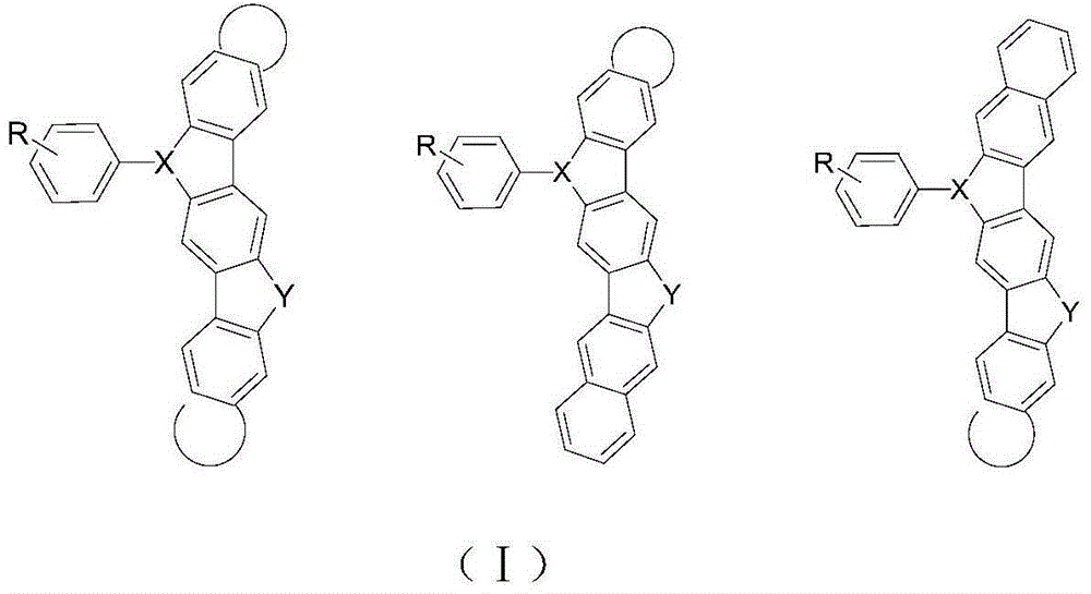
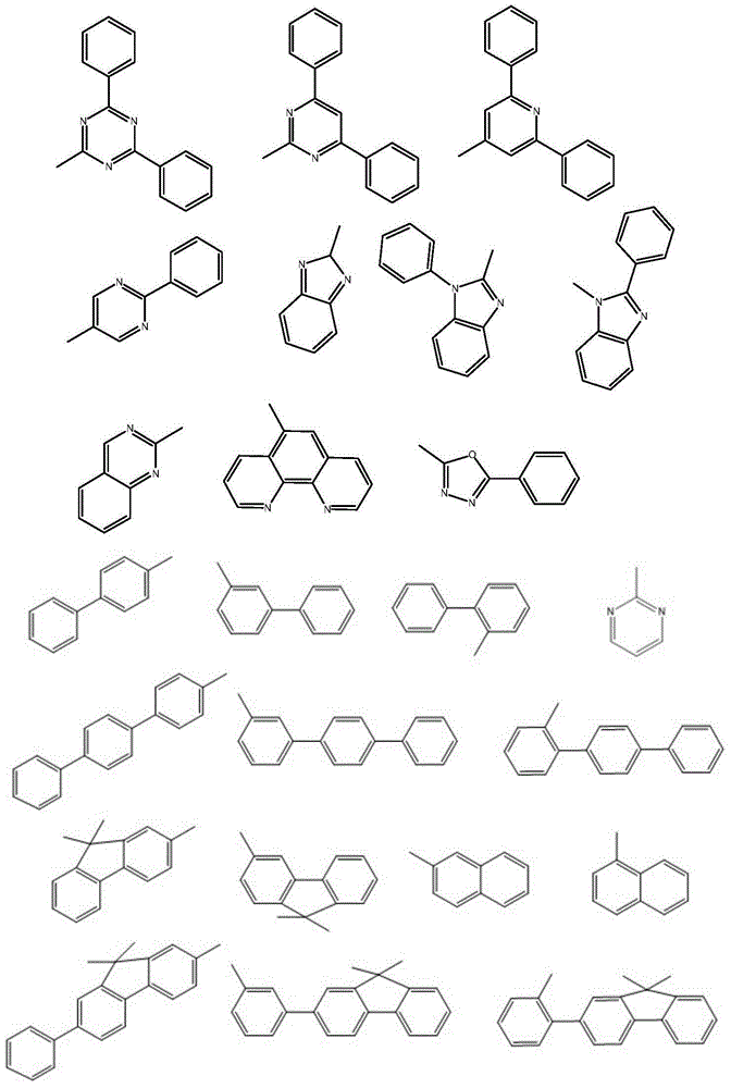
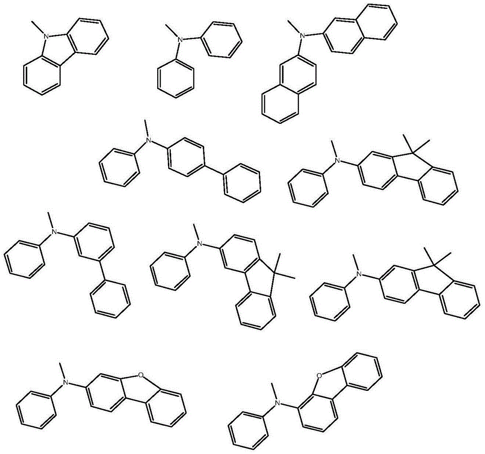
The invention provides an organic electroluminescent compound. The compound is characterized in that a structure of the compound is shown in a general formula (I), wherein X is N element, Y is N, S, O and Si element, and R is an aromatic group; R is the aromatic group which at least comprises C or at least comprises C and N; further preferably, R is the aromatic group which at least comprises three to twenty carbon atoms or at least comprises three to twenty carbon atoms and N atoms. The invention also provides an OLED electron transporting layer material, a luminescent layer material, and a hole transporting layer material, which separately comprise the compound shown in the general formula (I). The invention provides an OLED device which comprises the compound shown the general formula (I) and a preparation method thereof. The OLED material which comprises the compound shown in the general formula (I) is applied to the electron transporting layer material, the luminescent layer material, and the hole transporting layer material, so that the OLED display screen has effects of highlight brightness, high efficiency and low power consumption.

Description

technical field [0001] The invention relates to a compound, in particular to an organic electroluminescent compound and its application. Background technique [0002] At present, TFT (Thin Film Transistor, Thin Film Field Effect Transistor)-LCD is the main display screen. Since it is a non-self-illuminating display, light must be projected through the backlight and pass through the TFT-LCD panels in sequence. Polarizers, glass substrates, liquid crystal layers, color filters, glass substrates, polarizers and other related components must finally enter the human eye for imaging to achieve the display function. It is precisely because of the above-mentioned complicated display process that its display screen has shortcomings such as slow response rate, power consumption, and narrow viewing angle in the actual application process, which is not enough to become a perfect display screen. [0003] Relatively speaking, OLED is a new type of flat panel display technology. Compared ...

Claims


Application Information

Patent Timeline
Patent Type & Authority Applications(China)
IPC IPC(8): C09K11/06C07D495/04C07D491/048H01L51/54
Inventor 杨红领
Owner EVERDISPLAY OPTRONICS (SHANGHAI) CO LTD
Learn More