Determination method for interfacial photoelectron transfer and material photocatalysis activity, and four-dimensional microscopy imaging analyzer

A technology of photocatalytic activity and microscopic imaging, which is applied in the field of analytical chemistry, can solve the problems that cannot reflect, cannot reflect the change of interfacial photoelectron transfer and photocatalytic activity over time, and cannot identify unknown photocatalytic reaction products or intermediate products. Effects of Improving Detection Capabilities and Overcoming Detection Limitations

Active Publication Date: 2017-01-11
HUAZHONG NORMAL UNIV
View PDF5 Cites 3 Cited by
  • Summary
  • Abstract
  • Description
  • Claims
  • Application Information

AI Technical Summary

Problems solved by technology

This method cannot reflect the difference of a single photocatalytic active site of the material, and cannot identify unknown photocatalytic reaction products or intermediate products; (2) single-molecule fluorescence spectroscopy, which uses the target products produced by photocatalytic reactions (such as super Oxygen anions) and the fluorescence generated by probe molecules, although high-resolution fluorescence imaging of a single photocatalytic active site can be performed, but unknown photocatalytic reaction products or intermediate products cannot be identified; (3) Scanning electron microanalyzer, which This method requires the sample to be in a high vacuum state, so it cannot reflect the interfacial photoelectron transfer and photocatalytic activity and their changes with time under actual reaction conditions.

Method used


Image

  • Determination method for interfacial photoelectron transfer and material photocatalysis activity, and four-dimensional microscopy imaging analyzer
  • Determination method for interfacial photoelectron transfer and material photocatalysis activity, and four-dimensional microscopy imaging analyzer
  • Determination method for interfacial photoelectron transfer and material photocatalysis activity, and four-dimensional microscopy imaging analyzer

Examples


Embodiment 1

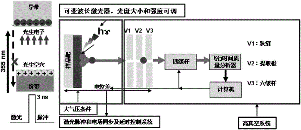
[0043] The method for measuring photoelectron transfer and photocatalytic active sites on the surface of titanium dioxide nanoparticles comprises the following steps:

[0044] (1) Preparation of titanium dioxide semiconductor nanomaterial suspension: Weigh 10 mg of nanomaterial and dissolve it in 1 mL of isopropanol, and ultrasonically oscillate for 1 minute to uniformly disperse the nanoparticles;

[0045] (2) Preparation of electron acceptor molecule solution: Weigh 100 mg of 5-hydroxy-1,4-naphthoquinone and dissolve it in 1 mL of acetone to prepare electron acceptor molecule solution;

[0046] (3) Clean the sample target, take 1 microliter of the titanium dioxide semiconductor nanomaterial suspension and drop it on the sample target, and let it dry naturally; get 1 microliter of the electron acceptor molecule solution and drop it on the surface of the titanium dioxide semiconductor nanomaterial, and let it dry naturally;

[0047] (4) Put the sample target into the four-dime...

Embodiment 2

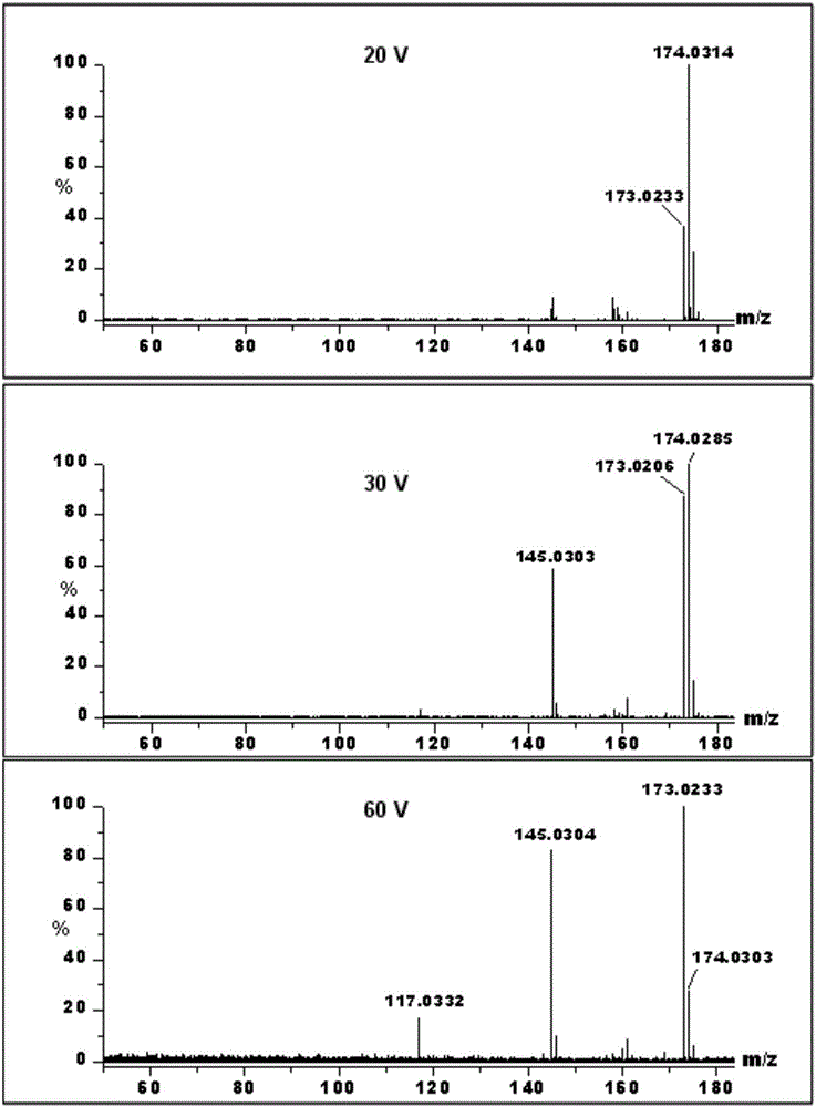
[0053] In this embodiment, the four-dimensional microscopic imaging analyzer is also switched to the positive ion detection mode, and the photoelectron transfer and photocatalytic active sites on the surface of titanium dioxide nanoparticles are measured. The specific method is the same as that of Example 1, except that: In the detection mode, the voltage difference between the sample target and the slit is designed to be 50V, and the obtained positive ion spectrum is as follows Figure 5 as shown, Figure 5 This shows that the electron acceptor molecule has undergone electron detachment.

Embodiment 3

[0055] In this example, the photoelectron transfer and photocatalytic active sites on the crystal face and side surface exposed by titanium dioxide are measured. The specific measurement method is the same as that in Example 1, the difference is that the preparation of the sample target: use 5-hydroxyl-1, 4-naphthoquinone solution soaked to cover the exposed crystal face and side of titanium dioxide, and fixed the exposed crystal face and side of titanium dioxide adsorbed with 5-hydroxy-1,4-naphthoquinone on the conductive metal aluminum strip Or copper strip; the voltage difference between the sample target and the slit is designed to be 20V. detected as Figure 6 shown, from Figure 6 It can be seen that the microscopic imaging signal of the exposed crystal plane of titanium dioxide is very low, indicating that the photocatalytic activity is poor, while its side (non- crystal plane) shows a very strong microscopic imaging, indicating that it has a higher photocatalytic ...


PUM

PropertyMeasurementUnit
concentrationaaaaaaaaaa

Abstract

The invention belongs to the field of analytical chemistry, and in particular relates to a determination method for interfacial photoelectron transfer and material photocatalysis activity, and a four-dimensional microscopy imaging analyzer. The four-dimensional microscopy imaging analyzer comprises a sample target, a laser, a slit, an extraction electrode, a hexapole, a quadrupole, a flying time mass analyzer, a detector and a device for supplying the sample target, slit, extraction electrode and hexapole with voltage. The determination method and four-dimensional microscopy imaging analyzer make use of the tunnel effect that a semiconductor material generates photoinduced electrons under laser illumination and the capture principle of electron acceptor molecules, determine the mass-to-charge ratio and ion signal of the interfacial transfer photoinduced electrons captured by the electron acceptor molecules or a product of photochemical reaction initiated by the interfacial transfer photoinduced electrons captured by the electron acceptor molecules, and obtain the microscopy imaging of a photocatalysis active spot through image reconstruction, thereby judging the photocatalysis active spot of the semiconductor material on the one hand, and judging the difficulty of the electron acceptor molecules in generating photochemical reaction and the product of photochemical reaction on the other hand.

Description

technical field [0001] The invention belongs to the field of analytical chemistry, and in particular relates to a method for measuring interface photoelectron transfer and material photocatalytic activity and a four-dimensional microscopic imaging analyzer. Background technique [0002] The photoelectron transfer at the heterogeneous interface is a key link in the photocatalytic reaction. The real-time monitoring of the heterogeneous electron transfer process and the determination of the intermediate transition state and reaction products of the photocatalytic reaction play an important role in understanding the conversion of solar energy and the photodegradation of environmental pollutants. At present, the measurement methods of interfacial photoelectron transfer and photocatalytic activity of materials include three categories: (1) Overall mean method, such as surface-enhanced Raman spectroscopy and fluorescence spectroscopy. This method cannot reflect the difference of a ...

Claims


Application Information

Patent Timeline
Patent Type & Authority Applications(China)
IPC IPC(8): G01N21/63
CPCG01N21/63
Inventor 钟鸿英张娟姜若葳张文洋唐雪妹
Owner HUAZHONG NORMAL UNIV
Why Eureka
Try Eureka