Method for epitaxial growth of crack-free high-crystal-quality LED epitaxial layer on metal gallium nitride composite substrate

A composite substrate and crystal quality technology, applied in semiconductor devices, electrical components, circuits, etc., can solve the problem of poor thermal conductivity of sapphire substrates

Active Publication Date: 2017-01-11
SINO NITRIDE SEMICON
View PDF8 Cites 11 Cited by
  • Summary
  • Abstract
  • Description
  • Claims
  • Application Information

AI Technical Summary

Problems solved by technology

However, the thermal conductivity of the sapphire substrate is not very good (about 25W / (m-K) at 100°C)

Method used


Image

  • Method for epitaxial growth of crack-free high-crystal-quality LED epitaxial layer on metal gallium nitride composite substrate

Examples


Embodiment 1

[0019] Use Aixtron company, tightly coupled vertical reaction chamber MOCVD growth system. During the growth process of the LED epitaxial wafer structure, trimethylgallium (TMGa), triethylgallium (TEGa), trimethylindium (TMIn), trimethylaluminum (TMAl) were used as Group III sources, ammonia (NH 3 ) as Ga, Al, In and N sources respectively, with silane (SiH 4 ) as an n-type dopant, dimagnesocene (Cp 2 Mg) as a p-type dopant;

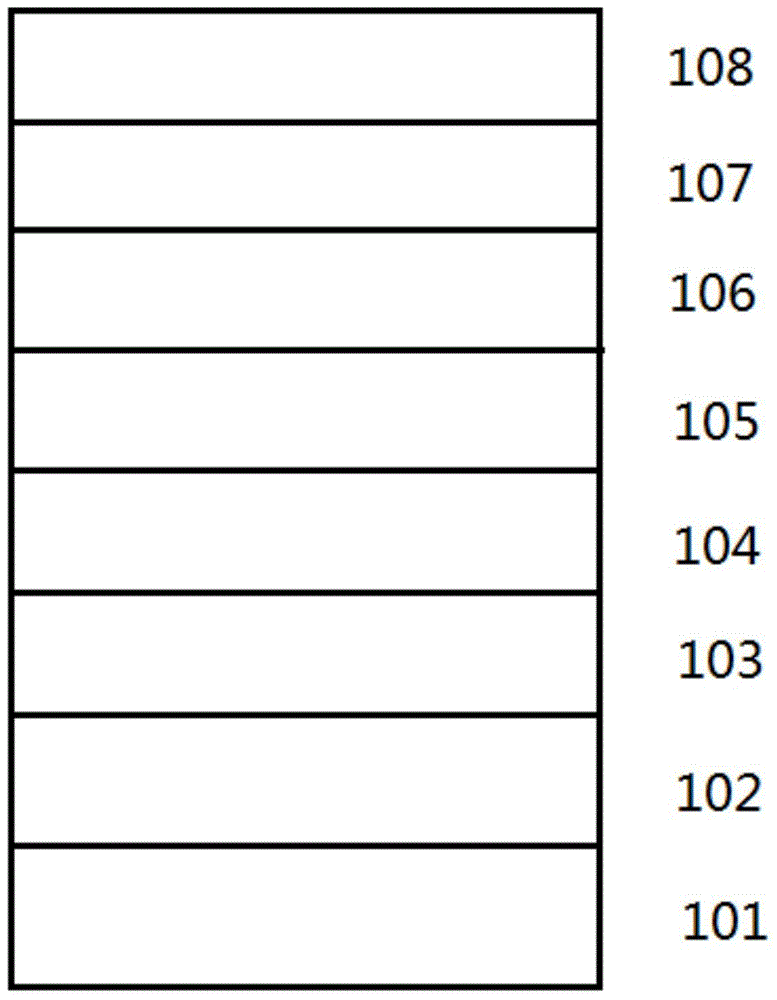
[0020] First in the metal organic compound vapor phase epitaxy reaction chamber the metal gallium nitride composite substrate (101), in nitrogen (N 2 ) atmosphere, the temperature was raised to 750-850°C for annealing treatment, and NH was slowly introduced into the reaction chamber after annealing treatment 3 , the NH 3 The flow rate increases sequentially: 1500sccm, 3000sccm, 6000sccm, 8000sccm, 10000sccm (sccm, standard cubic centimeter per minute, standard cubic centimeter per minute), and then slowly introduce TMGa, the pressure in the reaction ...


PUM

PropertyMeasurementUnit
thicknessaaaaaaaaaa
thicknessaaaaaaaaaa

Abstract

The invention discloses a method for epitaxial growth of a crack-free high-crystal-quality LED epitaxial layer on a metal gallium nitride composite substrate. The method comprises the steps of performing annealing treatment on the metal GaN (gallium nitride) composite substrate firstly in an N<2> atmosphere at a temperature of 750-850 DEG C at reaction chamber pressure of less than 300torr, and enabling a low-temperature GaN stress release layer with a thickness of 100-300 nanometers to be grown at a low speed of 0.2-1.0 micron/h; then enabling a high-temperature non-doped GaN buffer layer with a thickness of 1-2 microns to be grown at a variable speed linearly changed from 1 micron/h to 3 micron/h in an H<2> atmosphere at a temperature of 950-1,050 DEG C; next, enabling an n type GaN layer with a thickness of 1-2 microns to be grown at a constant growth speed; then enabling a multi-period InGaN/GaN multi-quantum-well active region to be grown in the N<2> atmosphere at a temperature of 750-850 DEG C; and next, enabling a p type AlGaN/GaN superlattice electron barrier layer and a p type GaN layer to be grown in the H<2> atmosphere at a temperature of 950-1,000 DEG C. According to the method, by optimizing parameters of carrier gas, growth temperature, growth speed and the like in the initial growth period of the metal substrate, thermal mismatch between the GaN epitaxial layer and the metal substrate can be effectively relieved to prevent decomposition of the GaN; and the high-quality GaN-based LED epitaxial layer is prepared on the metal substrate.

Description

technical field [0001] The invention relates to the technical field of semiconductor optoelectronics, and relates to a method for epitaxially developing an LED epitaxial layer with no cracks and high crystal quality on a metal gallium nitride composite substrate. Background technique [0002] People are paying more and more attention to the heat dissipation of LEDs. This is because the light decay or life of LEDs is directly related to its junction temperature. If the heat dissipation is not good, the junction temperature will be high and the lifespan will be short. Lowering the life by 10°C will prolong the life by 2 times. The relationship between light attenuation and junction temperature ( figure 1 ) can be seen, if the junction temperature can be controlled at 65°C, then the lifetime of its light decay to 70% can be as high as 100,000 hours! This is the lifespan people dream of, but is it really possible? Yes, it's possible to do that if you take care of its thermals...

Claims


Application Information

Patent Timeline
Patent Type & Authority Applications(China)
IPC IPC(8): H01L33/00H01L33/12H01L33/32
CPCH01L33/0062H01L33/12H01L2933/0008
Inventor 贾传宇殷淑仪张国义
Owner SINO NITRIDE SEMICON
Why Eureka
Try Eureka