Thin-film device based on GeSbTe phase-change material

A phase change material and thin film device technology, applied in the field of phase change storage, can solve the problems of poor thermal stability, poor crystallization speed, and short data storage life, improve thermal stability, avoid quality defects, and improve thermal stability. Effect

Active Publication Date: 2017-02-01
GUANGDONG UNIV OF PETROCHEMICAL TECH
View PDF2 Cites 8 Cited by
  • Summary
  • Abstract
  • Description
  • Claims
  • Application Information

AI Technical Summary

Problems solved by technology

However, the poor thermal stability caused by the low crystallization temperature and poor data retention of Ge-Sb-Te materials has been restricting its further development in special fields
In practical applications, GeSbTe storage materials have the following disadvantages: such as a large density change during phase transition, and the crystallization speed is not good, generally a few hundred ns, which affects the erasing speed and device reliability; for example, due to the low crystallization temperature (about 150°C), the data of PRAM memory cells using traditional Ge2Sb2Te5 materials as storage media can only be stored fo

Method used


Image

  • Thin-film device based on GeSbTe phase-change material

Examples


Embodiment 1

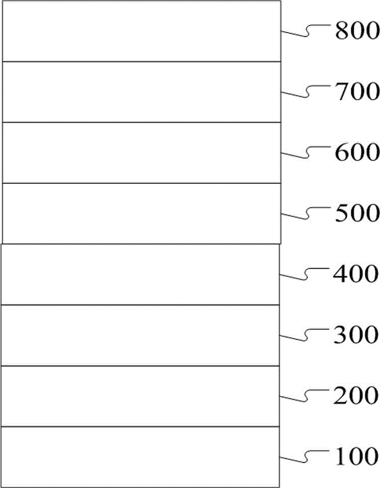
[0031] Such as figure 1 As shown, the present invention discloses a thin film device based on a GeSbTe phase change material comprising a substrate layer 100, a lower electrode layer 200, a first GeSbTe material layer 300, a molybdenum disulfide layer 400, a second GeSbTe material layer 500, and graphene Layer 600, upper electrode layer 700 and protective layer 800, the lower electrode layer 200, the first GeSbTe material layer 300, molybdenum disulfide layer 400, the second GeSbTe material layer 500, graphene layer 600, upper electrode layer 700, protective Layers 800 are sequentially deposited and superimposed on the substrate layer 100, the first GeSbTe material layer 300 is an ion-doped GeSbTe phase change material layer, and the second GeSbTe material layer 500 is a pure phase GeSbTe phase change material.

[0032] In this embodiment, the first GeSbTe material layer 300 is Ti 3+ Doped GeSbTe phase change material; the substrate layer 100 is a glass sheet; the protective la...

Embodiment 2

[0035] Such as figure 1 As shown, the present invention discloses a thin film device based on a GeSbTe phase change material comprising a substrate layer 100, a lower electrode layer 200, a first GeSbTe material layer 300, a molybdenum disulfide layer 400, a second GeSbTe material layer 500, and graphene Layer 600, upper electrode layer 700 and protective layer 800, the lower electrode layer 200, the first GeSbTe material layer 300, molybdenum disulfide layer 400, the second GeSbTe material layer 500, graphene layer 600, upper electrode layer 700, protective Layers 800 are sequentially deposited and superimposed on the substrate layer 100, the first GeSbTe material layer 300 is an ion-doped GeSbTe phase change material layer, and the second GeSbTe material layer 500 is a pure phase GeSbTe phase change material.

[0036] In this embodiment, the first GeSbTe material layer 300 is Ni 2+ Doped GeSbTe phase change material; the substrate layer 100 is a silicon wafer; the protectiv...

Embodiment 3

[0039] Such as figure 1 As shown, the present invention discloses a thin film device based on a GeSbTe phase change material comprising a substrate layer 100, a lower electrode layer 200, a first GeSbTe material layer 300, a molybdenum disulfide layer 400, a second GeSbTe material layer 500, and graphene Layer 600, upper electrode layer 700 and protective layer 800, the lower electrode layer 200, the first GeSbTe material layer 300, molybdenum disulfide layer 400, the second GeSbTe material layer 500, graphene layer 600, upper electrode layer 700, protective Layers 800 are sequentially deposited and superimposed on the substrate layer 100, the first GeSbTe material layer 300 is an ion-doped GeSbTe phase change material layer, and the second GeSbTe material layer 500 is a pure phase GeSbTe phase change material.

[0040] In this embodiment, the first GeSbTe material layer 300 includes Al 3+ Doped GeSbTe phase change material; the substrate layer 100 is a carbonate sheet; the p...


PUM

PropertyMeasurementUnit
Thicknessaaaaaaaaaa
Thicknessaaaaaaaaaa

Abstract

The invention discloses a thin-film device based on a GeSbTe phase-change material. The thin-film device comprises a substrate layer, a lower electrode layer, a first GeSbTe material layer, a molybdenum disulfide layer, a second GeSbTe material layer, a graphene layer, an upper electrode layer and a protective layer, wherein the lower electrode layer, the first GeSbTe material layer, the molybdenum disulfide layer, the second GeSbTe material layer, the graphene layer, the upper electrode layer and the protective layer are sedimented and laminated on the substrate layer in sequence; the first GeSbTe material layer is an ion-doped GeSbTe phase-change material layer; and the second GeSbTe material layer is a pure-phase GeSbTe phase-change material. The thin-film device based on the GeSbTe phase-change material disclosed by the invention has the characteristics of high heat stability, good consistency, high phase-change speed and long service life.

Description

technical field [0001] The invention relates to the field of phase change memory, in particular to a laminated phase change thin film device with complementary properties of multilayer materials. Background technique [0002] Phase-change memory (PRAM), as a non-volatile storage technology, has greater advantages in size reduction compared with FLASH technology. It not only has the characteristics of fast read and write speed (ns level), high cycle times (>1012), low power consumption, etc., but also is compatible with the existing CMOS process, the technical implementation difficulty and industrial cost are low, and it can realize Multi-bit storage. In addition, PRAM storage technology has strong shock resistance and radiation resistance, and has extremely important application prospects in the aerospace field. These characteristics of PRAM are considered to be the most likely to replace flash memory and become a new generation of non-volatile memory for general use. ...

Claims


Application Information

Patent Timeline
IPC IPC(8): H01L45/00
CPCH10N70/00
Inventor 朱伟玲陈星源古迪
Owner GUANGDONG UNIV OF PETROCHEMICAL TECH
Why Eureka
Try Eureka