
Glass chip packaging method

A glass chip and packaging method technology, which is applied in the manufacture of electrical components, circuits, semiconductors/solid devices, etc., can solve the problems of conductive leads and glass damage, limited packaging thickness, poor packaging performance, etc., and achieve excellent sealing performance and long service life The effect of unlimited length and chip thickness

Active Publication Date: 2017-02-22
HUAZHONG UNIV OF SCI & TECH
View PDF5 Cites 26 Cited by
  • Summary
  • Abstract
  • Description
  • Claims
  • Application Information

AI Technical Summary

Problems solved by technology

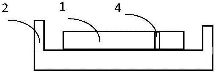
[0011] In view of the above problems, the present invention provides a glass chip packaging method, which directly melts the material of the glass itself by an ultrafast laser to realize chip packaging, improves the strength, sealing, stability, reliability and prolonging the life of the package to solve the problem of current problems. There are problems such as conductive leads and glass in glass packaging technology are easily damaged by laser, limited packaging thickness, and poor packaging performance

Method used


Image

  • Glass chip packaging method
  • Glass chip packaging method
  • Glass chip packaging method

Examples


example 1

[0059] Example 1: Fabrication of glass perovskite solar cell chip packaging

[0060] Put the crucible mold with the first flat glass substrate with a thickness of 1mm, length and width of 20mm and 15mm respectively into a high-temperature heating furnace, raise the temperature evenly to 550°C to soften the first flat glass substrate, and take out the crucible mold . Quickly insert two copper wires with a diameter of 1 mm into the first flat glass substrate to soften, allowing the copper wires to penetrate through the glass sheet to soften. Then put the crucible mold into a high-temperature heating furnace, raise the temperature to 700°C, and stay for 3 minutes, so that the glass sheet and the copper wire are fully and closely contacted to achieve the sealing condition. After slowly lowering the high-temperature heating furnace to room temperature, a penetrating conductive metal electrode penetrating through its thickness and having good sealing properties is obtained on the f...

example 2

[0061]Example 2: Encapsulation of glass biochips

[0062] Put the crucible mold with the first flat glass substrate with a thickness of 1mm, length and width of 20mm and 15mm respectively into a high-temperature heating furnace, raise the temperature evenly to 550°C to soften the first flat glass substrate, and take out the crucible mold . Quickly insert two copper wires with a diameter of 1 mm into the first flat glass substrate to soften, allowing the copper wires to penetrate through the glass sheet to soften. Then put the crucible mold into a high-temperature heating furnace, raise the temperature to 700°C, and stay for 3 minutes, so that the glass sheet and the copper wire are fully and closely contacted to achieve the sealing condition. After the temperature is slowly lowered to room temperature, a penetrating conductive metal electrode penetrating through its thickness and having good sealing performance is obtained on the first flat glass substrate. Prepare a biochip...

example 3

[0063] Example 3: Fabrication of Glass Organic Light Emitting Diode (OLED) Chip Packaging

[0064] Put the crucible mold with the first flat glass substrate with a thickness of 1mm, length and width of 10mm and 8mm respectively into a high-temperature heating furnace, and raise the temperature evenly to 500°C to soften the first flat glass substrate, and take out the crucible mold . Quickly insert two copper wires with a diameter of 2 mm into the first flat glass substrate to soften, allowing the copper wires to penetrate through the glass sheet to soften. Then put the crucible mold into a high-temperature heating furnace, raise the temperature to 700°C, and stay for 3 minutes, so that the glass sheet and the copper wire are fully and closely contacted to achieve the sealing condition. After the temperature is slowly lowered to room temperature, a penetrating conductive metal electrode penetrating through its thickness and having good sealing performance is obtained on the fi...


PUM

PropertyMeasurementUnit
Thicknessaaaaaaaaaa

Abstract

The invention discloses a glass chip packaging method. A penetrating conductive metal electrode is prefabricated in the thickness direction of a glass sheet, and laser welding packaging is carried out on a glass chip by adopting ultrafast laser light. By using an ultra-high light intensity characteristic of ultra-short pulse laser light, a nonlinear absorption effect is generated in a transparent medium and the transparent medium is melted on a focus point, so that selective micro-welding in a transparent material space is achieved. The structure size processed by the ultra-short pulse laser light can break through an optical diffraction limit and precise welding smaller than a laser wavelength is achieved. Furthermore, the interaction time of the laser light and a material is extremely short, cracks and sputtered materials, caused by different expansion coefficients, of the material can be effectively avoided; and improvement of the welding packaging precision and quality is facilitated. Compared with other packaging technologies of bonding and the like, the glass chip packaging method has the advantages that the manufacturing process is simple, the thickness of the chip is not limited, fillers of different materials do not need to be added, the strength performance, the stability and the reliability of glass chip packaging can be improved and the service life of the glass chip is prolonged.

Description

technical field [0001] The invention belongs to the technical field of chip packaging applications, and in particular relates to a glass chip packaging method. Background technique [0002] Glass materials are excellent materials for chip packaging such as implanted microelectronics, solar cells, organic light-emitting diodes (OLEDs), micro sensors and converters, and optoelectronic devices. They have great potential in electronic semiconductors, biomedicine, solar cells, aerospace and other fields Extremely extensive and potential application value and market prospect. This is because the glass material has many advantages: for example, the glass material can be regarded as a "neutral" substance for the living body, and when it is implanted into the human body, it has good biocompatibility with the body fluid tissue and will not immune rejection. Second, the glass material is not corroded by body fluids or spontaneously degrades like many adhesives or other additional sub...

Claims


Application Information

Patent Timeline
IPC IPC(8): H01L21/56
CPCH01L21/56
Inventor 段军张菲熊伟曾晓雁
Owner HUAZHONG UNIV OF SCI & TECH
Learn More